This thread has been locked.

If you have a related question, please click the "Ask a related question" button in the top right corner. The newly created question will be automatically linked to this question.

TLV431: Output Noise reduction

Part Number: TLV431
Other Parts Discussed in Thread: TLVH431, LM2903B, LM2903

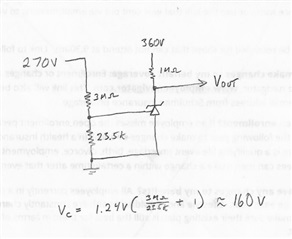
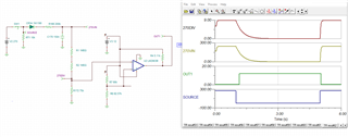
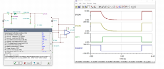
I am using the TLV431 in my design as a comparator. Note that there is a 8V Zener at Vout.  When the 270V input line powers up slowly, Vout initially goes low, but then goes high (8V) before it reaches the cutoff voltage, 160V. When 270V pass the trigger point of 160V, Vout goes low again at about 0.8V.  The problem I am having with this design is when I slowly power down and approach 160V, Vout becomes very noisy from 166 to 160v before Vout goes low. I realize that TLV431 does not have a Hysteresis feature, but before I add one to this circuit, I need to understand why so noisy within 166v to 160v.  The transition does not happen quick from low to high on Vout. Seems that the output transistor of the TLV431 does not saturate quickly at 160V or the pull down is very weak going to the trigger point. I tried lowering the current limiting resistor of 1Meg  to 500k ohms, but I see no change.  The datasheet shows a recommended operating range  between 0.100 to 15 mA. Using a limiting 500Kohm resistor, my cathode current is 720uA. Any help is appreciated.

  • Question on this part is TLVH431 and not TLV431.

  • Hi Luis 

    Couple of questions -

    • Do you have any capacitor at the Vout or reference pin? 
    • I am not sure if zener is causing some issue , can you lower down 360V supply to <=18V, or 8V  bias IKA =  720uA and check the performance if it is same ? 
    • Can you also share the picture of the noisy supply > is it oscillating at some perticular frequency? 

    Regards

    Trailokya 

  • Hi Trailokya,


    The attachment shows a better schematic of the circuit I am working on using the TLVH431.


    1. There are no capacitors at Vout or reference pin.
    2. The Zener is not 8V(my mistake), but 13V (CR36 and CR37)
    3. I can’t lower the 360V. A 13V source is created from the 360V using the CR36 and CR37 zeners.
    4. I am using a lab power supply that I use to vary down the voltage starting from 270VDC (simulating a 270V power down condition). The attached scope picture shows the noise (bottom green trace) when I am close to the 160V trigger point of TLVH431. The output of TLVH431 (CR30) is used to enable a power module which can be damaged by the noise. There are various circuit elements between the TLVH531 and the power module. The power module sees the top orange trace. The oscillation is occurring at 2.5 Hz.


    Luis TI Support - SCH.pdf

  • Also, looking at the datasheet of the TLVH431, I notice 4 things.

    First:

    9.2.1.2.1 Basic Operation In the configuration shown in Figure 24, TLVH431 behaves as a comparator, comparing the Vref pin voltage to the internal virtual reference voltage. When provided a proper cathode current (Ik ), TLVH431 will have enough open loop gain to provide a quick response. With the TLVH431's max Operating Current (Imin) being 100 uA and up to 150 uA over temperature, operation below that could result in low gain, leading to a slow response.

    MY RESPONSE: My Ik = 750uA. I should be OK since this higher than 150uA

    Second:

    9.2.1.2.2 Overdrive For minimal voltage drop or difference from Vin to the ref pin, it is recommended to use an input resistor ​it is recommended to use an input resistor ​​<10kohms to provide Iref.

    MY RESPONSE: I am using divider resistors to the reference pin 3Mohms and 23.5kohms. The equivalent resistance to the reference pin is 23.32kohms which is more the 10kohms.  Should I change the values so that the divider resistors combination will give me less than 10kohms.

    Third:

    9.2.1.2.3.1 Input Resistance TLVH431 requires an input resistance in this application in order to source the reference current (IREF) needed from this device to be in the proper operating regions while turning on. The actual voltage seen at the ref pin will be VREF = VIN – IREF × RIN. Because IREF can be as high as 0.5 µA, TI recommends to use a resistance small enough that will mitigate the error that IREF creates from VIN.

    MY RESPONSE: Is this similar to paragrapgh 9.2.1.2.2 (above).

    Fourth:

    9.2.2.2.3 Stability Though TLVH431 is stable with no capacitive load, the device that receives the shunt regulator's output voltage could present a capacitive load that is within the TLVH431 region of stability, shown in Figure 15, Figure 16 and Figure 17. Also, designers may use capacitive loads to improve the transient response or for power supply decoupling. TI recommends to choose capacitors that will give a phase margin > 5° to guarantee stability of the TLVH431.

    MY RESPONSE: From the figure shown on the datasheet (SLVS555L), it seems I don't have to add capacitance at the cathode. At Vka = 13V, I should be OK.

  • Hi Luis

    Thanks for detailed.

    • I dont think there is some stability issue, it looks more like bias point issue between the Zener and TLVH431. 
    • Can you please show the trace which has been probed at the TLVH431 output of what is the relation between the yellow trace and TLVH431 ?
    • I also  want to highlight one point that TLVH431 will be taking around 100uA of current when the the input at REF pin is close to 1.24 even if the device is off. Hence you need to check the knee current of the diode and see if that is able to regulate properly. 
    • Also Can you please confirm that you have bought the parts from authorized TI vendor ? Can you tell the exact part number? 

    Regards

    Trailokya 

  • Hi Trailokya,

    Thank you for your feedback.

    • I dont think there is some stability issue, it looks more like bias point issue between the Zener and TLVH431. 

                MY RESPONSE: What do you suggest?

    • Can you please show the trace which has been probed at the TLVH431 output of what is the relation between the yellow trace and TLVH431 ?

                MY RESPONSE: The bottom attachment shows the source of the traces. I can't show the detail in the power circuitry.

    • I also  want to highlight one point that TLVH431 will be taking around 100uA of current when the the input at REF pin is close to 1.24 even if the device is off. Hence you need to check the knee current of the diode and see if that is able to regulate properly. 

               MY RESPONSE: Thank for the highlighted point about the 100uA. I will lower the pull up resistor, R177 and R2 combination, from 500kohm to                      333kohms and lower the resistance on R1, too.

    • Also Can you please confirm that you have bought the parts from authorized TI vendor ? Can you tell the exact part number? 

               MY RESPONSE: The exact part number is: TLVH431IDBZT. Our purchasing staff are usually careful ordering parts from an authorized vendor, but I             will check.

    TI Support - SCH1.pdf

  • Hi Luis 

    Thanks for your response and sharing the schematic.  

    Can you please tell the puspose of CR133, as it will isolate EN from TLVH431 when OV event occurs. 

    Can you please test below circuit once if stability of 360V supply is better than noise margin of Power circuitar enable 

    • Short CR33 and CR36 diode and open CR37. 
    • Put R177 = 1Meg , R178 = 40 k ohms , open C171 , R1 and R2. 

    Plot the same waeform once again. I just want to confirm that the random waveform is due to the addityional setup.  Once confirmed, can yoy please check your circuit withot CR33. 

    Regards

    Trailokya 

  • 1. Yes. Good point. I also don't see the purpose of CR33. This was a leftover from a different version of this circuit. I will short it out.  With CR33 removed, R1 serves no purpose, too. Thanks.

    2. CR36 may be necessary since the EN line has a NPN bipolar transistor before the power circuitry that may not turn off completely at "OUT2".  When TLVH431 is low, "OUT" can be as high as 1.2V and that may not be low enough to turn off the NPN bipolar transistor (Vbe needs to be less than 0.7V to turn off).

    3. The 360V line can exceed 360V. I've seen it go just above 400V.  CR37 is more for protection in that it assures the voltage will not exceed 14V  on TLVH431 with CR36 and CR37 included. 

    On your previous message, you were concern with the effect derived from the zeners which maybe causing the noise on the TLVH431's Cathode.  Just to verify that, I will try out your suggestion.   

    • CR36 diode and open CR37. 
    • Put R177 = 1Meg , R178 = 40 k ohms , open C171 and R2.

    Thank you

    Luis

  • End of the day update :  I made all the changes per your recommendation.  Unfortunately, the power circuitry oscillated over a wider range while varying down the  270V lab power supply input. The power circuitry now oscillate from 190V down to 158V.  Before it oscillated from 166.7V to 165.6V.  I think part of the problem is the TLVH431 (when it's ON) does not bring the voltage low enough to the input of NPN bipolar transistor going to the power circuitry.  The lowest the TLVH431 will go is 1.2V. When the TLVH431 is OFF, the "OUT" will only transition high to about 0.8V due to the input of the bipolar NPN transistor.  To make a descent transition to the NPN Bipolar transistor without using the 2 previous zener, I have to figure another approach. 

  • Hi Luis 

    VOL for TLVH431 will be in the range of 0.8 to 1V . 

    We have voltage supervisor ICs  which have programable threshold (adjestable option) and open drain output which will have VOL close to 0V . 

    You can look into TPS3899DL01DSE part is has 0.505V threshold (you can adjust your resistor ladder) and VOH with some zener diode . 

    Please let me know if you have additional questions 

    Regards

  • I tried to use the LM2903B spice model from TI and input the MACRO on the TINA schematic.  The part is supplied with 12V and a divider (also using the 12V) is on the noninverting input of LM2903 triggering point at 6V (100k/100k divider).  I connect a 12V to an RC circuit and connect that to the inverting input of the LM2903. When I run the TINA simulator, LM2903 triggers between the rail voltage 12V and GND, but not at 6V.  Am I using the macro incorrectly? 

  • Hi Comparator team 

    Can you please respond to the query. 

    Regards

    Trailokya 

  • Hi Luis,

    Can you send me your tina sim file?

     Most likely the issue is that you are violating the input common mode range (VEE to VCC - 2V). In this case we have the model give out an error condition by going to mid supply when the common mode range spec is violated. This does not happen in the real device

  • Hi Luis,

    The model is working as intended. I am not sure I am following what your issue is. "270DIV" drops below the reference voltage of 5.74V at IN+ in which the comparator goes HIGH at 12V. "270DIV" swings above 5.74 and the comparator goes LOW, close to GND. Can you explain what you were intending it to be?

    I would also consider increasing the pull up resistor size, 12V with a 5k resistor would burn more power and increase the risetime and timing of your circuit. 12kohm or more would be good. 

    I also see a floating 1MEG resistor at R3. Was this supposed to be connected?

  • Hi Chi,

    Thank you for the feedback. Actually, I ran the TINA simulator, again and it runs fine. Not sure what happen, but I have another question. When I ran the simulator, the waveform I got for the "SOURCE" has a slow rise time (about 90ms). Is there a way to reduce the rise time similar to the fall time for the "SOURCE" waveform? See the simulation output for the file I sent you in the previous message.

  • Hi Luis,

    I believe the fall time and the rise time is affected by the charging/discharging of your RC network of R166 and C170 (RC time constant). Consider playing around with the values, such as increasing R to 200kohm.

  • "SOURCE" is connected before the RC network. Not after. I understand the Fall time, but not the rise time. No problem. I am using LTSPICE and is does not exhibit this behaviour. Thanks anyway.

  • Hi Luis,

    Here is what I got. But of course this would change your divider voltages. It may also have to do with the switch. But I am glad you didnt see the issue in LTSpice. Thanks. 

  • Sorry Luis, found it was also a TINA related issue. Here I changed the TR max time step, since you simulated for 6 seconds, i set the time step to 6ms and got better results with the original 10kohm resistor. 

  • Thanks. I will try it on TINA