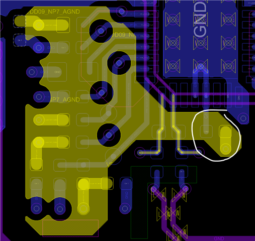
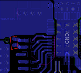
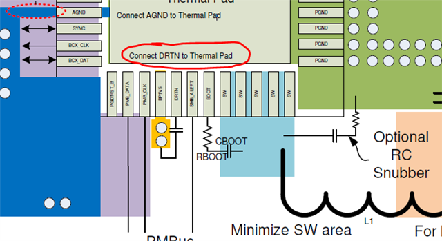
1. due to some reason, can they connect AGND to NC first and then use NC pin to connect to thermal pad?
I assume NC doesn't connect to anything so should be flexible, right?
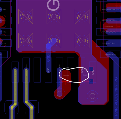
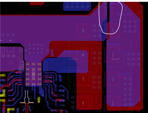
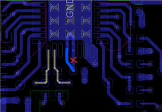
2. there's a conflict there, pin definition said don't connect anything to DRTN but layout example says differently,
please guide us the right direction
3. regarding power sequence, can AVIN power up before PVIN if these two are separate ?