This thread has been locked.

If you have a related question, please click the "Ask a related question" button in the top right corner. The newly created question will be automatically linked to this question.

TPS544B25: Crossover frequency and phase margin selection for stable loop

Part Number: TPS544B25


Hi Team,

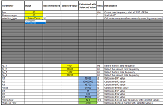
I am not sure how to select the FCO value for compensation circuit used for TPS544B25.I have read online that it should be FSW/10 or FSW/5.Can you please tell what is the thumb rule to select the FCO and pahse margin for stable loop compensation circuit.

  •  

    Between Fsw/10 and Fsw/5 with 45-60 degrees of phase margin would be the general rules of thumb.

    Fsw / 10 is generally conservative and tolerant to parasitics like layout resistance and inductance,  while Fsw / 5 is more aggressive and requires more care with the actual ESR of components.

    Also, watch for the loop response phase dropping at the L-C resonance, especially in designs that use all ceramic output capacitors and low DCR inductors.  These under damped resonant systems can have the loop phase drop very low.  This does not cause steady-state instability, but can result in the output voltage oscillating during Output Voltage changes, such as soft-start or during VOUT_COMMAND changes for AVS.

    If you see the Loop Phase drop below 35 degrees at the L-C resonance frequency, I would recommend using the "Set Pole and Zero" frequencies option and adjust the zero frequencies so that the first zero is 1/2 the L-C resonant frequency and the second is about 90% of the L-C Resonant frequency to get more phase boost before the L-C resonance.

    Alternately you could manually double C3, which will reduce its zero frequency by 1/2 without changing the gain above the Zero or the pole frequency.

  • If you see the Loop Phase drop below 35 degrees at the L-C resonance frequency, I would recommend using the "Set Pole and Zero" frequencies option and adjust the zero frequencies so that the first zero is 1/2 the L-C resonant frequency and the second is about 90% of the L-C Resonant frequency to get more phase boost before the L-C resonance.

    How can we check this in excel sheet or graph?

    I had tried to do simulation of TI PSPICE MODEL which is availble on TPS544B25 web page.I am seeing Ripples on VOUT and Pulse skipping on Switching Node.May i know is this modeling issue or somethings else is bothering the simulation.

    Note- Startup model is working fine.

  •  I have attached the image of Trasient simulation.

  • Hello Raja, 

    Can you please provide the SCH, we can review, I am sure it is just tuning of the COMP. Also fill up the calculation tool please.

    Thanks 

    Tahar

  • Hi Allag,

    I did not change anything in TI default Transient scheamtic which i have downloaded from TI website.Here is the snap.

    Many Thanks

    Rajat

  • Hi Rajat,

    I will cover for Tahar and Peter since they are OOO today.

    I downloaded the PSPICE model from the TI website, and I was able to run the Transient Load simulation without any issues:

    While you said you hadn't changed the TI default, the load step has changed in your simulation result. For example, TI default has a 20A load step, but yours is 10A.

    Is there anything else you have changed so we can reproduce it on our end?

    Thank you,
    Tomoya

  • Also, watch for the loop response phase dropping at the L-C resonance, especially in designs that use all ceramic output capacitors and low DCR inductors.  These under damped resonant systems can have the loop phase drop very low.  This does not cause steady-state instability, but can result in the output voltage oscillating during Output Voltage changes, such as soft-start or during VOUT_COMMAND changes for AVS.

    If you see the Loop Phase drop below 35 degrees at the L-C resonance frequency, I would recommend using the "Set Pole and Zero" frequencies option and adjust the zero frequencies so that the first zero is 1/2 the L-C resonant frequency and the second is about 90% of the L-C Resonant frequency to get more phase boost before the L-C resonance.

    How can i check this ?

  •  

    The TPS544B25 excel design calculator, available from the TPS544B25 product folder  - https://www.ti.com/product/TPS544B25#design-tools-simulation includes a graphic representation of the predicted bode plot.

    By selecting a low inductor DCR, low capacitor ESR and low output current, you can the phase drops rapidly at L-C resonance, before the two zeroes of the Type-III compensation can boost the phase.  To lower one of the zeros and boost the phase before the L-C resonance, without increasing the loop bandwidth, increase the value of C2 

    Increasing C2 from 820pF to 3900pF lowers the zero and provides the needed phase boost before the L-C resonance.

    To use the Pole-Zero frequency selection for compensation design, select "Pole / Zero" for Selection Type in Cell C89.

    Following the guidance of Fz_1 = 1/2 LC resonance, Fz_2 = 0.9x LC resonance, Fp_1 = lower of ESR zero frequency or 1/2 switching frequency, and Fp_2 = switching frequency.  

    We can see that even under the extreme conditions we have been following here, the phase is maintained near 45 degrees at L-C resonance

  • Hi Peter,

    Very well explained thanks.

    so F_LC will be the resonance frequency and we have to check the Phase on this frequency right ? I have marked in circle please confirm.

    As per my understanding from your explanantion Phase should not fall below 35 degree right in "total system bode plot"

    Please confirm

  •  

    Yes, F_LC is the resonance frequency of the L-C power stage.

    Yes, you should check the "Total System Bode Plot" graph, wish is the full voltage regulation loop from VOUT going into feedback to VOUT coming out of the inductor.

    It's not specifically at the resonance frequency that we are concerned about, but the valley of the phase plot, which will occur slightly above the resonance frequency - about 13k in the above example.

    For this particular test, I like to set the Io to 1/2 the inductor peak to peak ripple - also called critical conduction, as this is the load current were the damping on the L-C resonance is the lowest and the phase shift from the resonance the worst.

    35 degrees is not a "hard" rule, but a general rule of thumb.  Lower phase margins at L-C resonance will tend to cause the output voltage to oscillate at that frequency when high gain is needed from the loop at that frequency, such as tracking a change in the reference voltage due to soft-start or AVS change in VOUT_COMMAND, or during recovery from a large loading transient.