This thread has been locked.

If you have a related question, please click the "Ask a related question" button in the top right corner. The newly created question will be automatically linked to this question.

UCC28070A: UCC28070 Abnormal PFC waveform

Part Number: UCC28070A

Dear Sir

Power output: 5KW
Input voltage range: 165-270 VAC
PFC voltage: 410Vdc
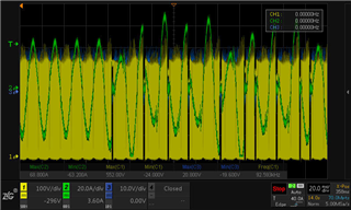
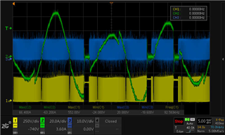
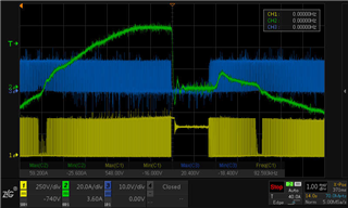
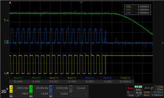
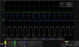
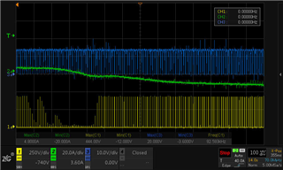
Abnormal recurrence: with full load, voltage from high voltage to low voltage test input undervoltage protection,
When the voltage is about 180Vac, the power factor drops to about 0.86 and the input current distorts.
As shown below: (1# waveform is DS waveform, 2# is input current waveform, and 3# is GS drive waveform)

  • Hello Gabriel, 

    There appear to be a number of things happening here.  
    First, the slow steady decrease of input voltage to ~180Vac leads VINAC to drop through a low-going feed-forward threshold (Vff) to increase the multiplier gain.
    (When Vin is high, input current should be low, so gain is low.  When Vin is lower, input current should be higher, so gain is higher.)

    The change in multiplier gain is a step change which can be seen as a sudden increase of input current just after the current peak in the 2nd waveform. 
    This increase in current charges the PFC output capacitor more rapidly than the load can absorb, and the voltage-loop response is slow to reduce it, so Vout rises to the 106% over-voltage threshold and switching stops due to OVP response.  This can be seen as flat gaps in the current for 1~2ms.  Switching resumes when the OV subsides by about 3%.  

    During the switching time, the high load drops some voltage across the input source impedance. During the non-switching time, the input source voltage pops back up and the VINAC rises through an up-going threshold to change the multiplier gain to a lower level.  Then when the switching resumes and input current rises, the source impedance drops Vin again so that VINAC falls back down to the next lower Vff level which raises the multiplier gain and the input current increases again.
    This overcharges Cout and Vout rises to hit OVP again and the cycle repeats. 

    This is what causes the repeated current distortions and low PF around ~180Vac.  Further reduction of Vin below ~180Vac should get past this threshold and settle to a nromal steady-state of operation.  However, the same thing may happen at a lower input voltage at the next Vff threshold. 

    There are some countermeasures that can be done for this situation:
    1.  Increase Cout so that the ΔV at each Vff level change is smaller and does not trigger the 106% OVP threshold. 
    2.  Reduce the total source impedance which includes the Zout of the voltage source itself plus the voltage drops of the EMI line filter and input diodes and other series resistances.
    3.  Relocate the sense point of VINAC from Cin to reconnect earlier in the AC source path, before the series impedance voltage drops. This may not solve the OVP, but can help avoid toggling the multiplier gain up and down and avoid the repeating disturbances. 
    4.  Add a "voltage-compression" circuit to VSENSE to effectively raise the OVP threshold by reducing the feedback divider gain as Vout nears the normal OVP level. (This is a complicated solution.) 

    These countermeasures may be done individually or in combination. You can try each one to see which are preferable. 

    Regards,
    Ulrich