This thread has been locked.

If you have a related question, please click the "Ask a related question" button in the top right corner. The newly created question will be automatically linked to this question.

LM5085: Poor load regulation, and premature current limiting

Part Number: LM5085
Other Parts Discussed in Thread: LM5145

Hi All,

I've been working on a SMPS design using the LM5085. We have a potentiometer in the feeback loop, so Vout is variable between 32.4 and 46 V, and Iout is supposed to be up to 7.5 A.

1) The load regulation isn't great. It's better at the low Vout, but it's really poor at high Vout. Vout is down to 42 V (it's supposed to be 46 V) by the time the load is 3.2 A, and it falls fast from there. This will be driving an enormous LED array, which is pretty much a fixed load, so we don't need fantastic load regulation, but at higher voltages, it will be driving a higher current.

2) The bigger problem is that at about 4 A, Vout drops significantly, and by 4.2 A it drops to 0 V. This is obviously a big problem. We probably won't need to drive to 7.5 A, but I've designed it as such for a little wiggle room, so I'd like it to operate as such. Can anyone assist me with this?
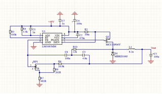
  • So I increased the value of R4 (Radj), and that seems to have helped the current limiting issue, however the load regulation is still very poor. Vout should be 44 V, but at a 3.5 A load, Vout is 41 V. At 4 A, Vout is 38 V. At 4.5 A, Vout drops way down to 30 V. At 5 A, Vout is 28 V.

    The regulator is not keeping FB at 1.250 V. Even at a relatively paltry 0.5 A load, its at 1.205 V. By the time the load gets to 2 A, FB is 1.177 V, by 3 A, FB is 1.095.

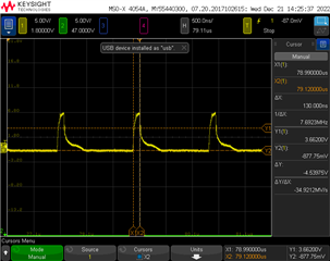
    I probed the gate signal, and it looks like the duty cycle is about 90% throughout the entire load range (with Vout set to the maximum value). This regulator should be capable of 100% duty cycle, but it doesn't seem like it is in order to bring FB back up to 1.25 V. Ohmic losses across the Rsens, Q1, and L1 don't account for the marked drop in Vout (also, those would be linear).

    My gut is telling me that the issue is with C3, C6 and R10, but I'm not sure what to do.

    Thank you!

  • I guess the numbers that I used to calculate the values for C3, C6 and R10 would probably help you.

    VA = Vout-(0.65*(1-Vout/Vin)

    Vout = 46 V, Vin = 48 V

    VA=45.97V

    fsw = 712 kHz (I measured this at about 694 kHz, so it's not far off)

    ton = Vout/(Vin*fsw) = 1.34 us

    R10*C3 = (Vin-Va)*ton/delV

    delV = 0.025

    R10*C3 = 109e-6

    R10 = 22 kO

    C3 = 4.96 nF, rounded down to 4.8 nF

    One thing I will note is that there is very little voltage ripple. I'm not sure whether that is relevant. I've also attached a screenshot with the gate signal.

  • Hi Alexander,

    I recommend minimizing the number feedback resistors as FB is a noise-sensitive node. As such, the FB trace should be as short as possible, and the feedback resistors should be right at the IC.

    Note this seems quite a high switching frequency for a high Vin(48V) application. I recommend using ceramic input and output caps, not electrolytic, at this frequency. In general, 250-350kHz is a better tradeoff of size and efficiency. You can use the quickstart calculator (available by download from the product folder) to assist with component selection.

    Regards,

    Tim

  • Hi Tim,

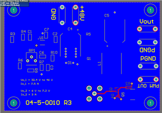
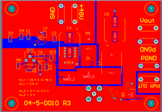
    Unfortunately we need a variable power supply, and this was the minimum number of resistors that would give us the range and sensitivity that we require. I'm using a mechanical potentiometer for the prototype, but the final design will use a digital potentiometer, which is much smaller than a mechanical one. The output plane convers the right and bottom side of the board (you can see it on the top layer).

    Reducing the switching frequency would require an extremely large resistor. I can put a 1 MO resistor in place of the 430k, which would bring the frequency down to 300 kHz.

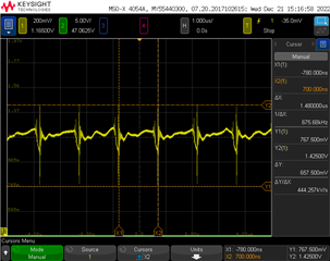
    I probed FB, and the noise doesn't seem to be a function of load, although it isn't small. I've attached a screenshot.

    I'll try bringing the switching frequency down.

    I did make an interesting observation. I set the load to 5 A and rotated the potentiometer to get the lowest output voltage. At that load, Vout increased as I rotated the potentiometer until it was nearly at its extreme, when it dropped suddenly. That does not sound like a noise problem, but I don't know what it does sound like.

  • Hi Tim,

    Changing Rt to bring the switching frequency down worked wonders! I'm going to finish the validation now, but I got up to 5 A without any drop in Vout. I think I need to make Radj even larger, since I'm still not getting to 7.5 A, but that's an easy change.

    Thank you!

  • This likely confirms it's a noise issue - it's very important to locate the feedback components really close to the FB pin. Also, layer 2 of the PCB (directly under the IC and power stage, should be a solid GND plane.

    With the lower Fsw, you will likely need a higher inductance to maintain 30-40% ripple current for best losses. Use the quickstart file to derive component values.

    Regards,

    Tim

  • Hi Tim,

    The bottom plane is a solid ground plane. I think we can deal with higher current ripple, although I'll look into other inductors. Earlier today, I switched out Rt with a 4.7 kO resistor. That raised the current limit to 5.2 A. I switched that out with a 6.8 kO resistor in hopes to bring it up even further. Much to my surprise, the current limit didn't change. It still shut off at 5.2 A. Do you have any insight as to how I could increase the current limit? Would I need to decrease Rsense? Given that I don't really care about current limiting, could I replace Rsense with a 0 O jumper?

    Thank you!.

  • Can you probe the voltage across the shunt resistor and at the pins of the IC (VIN and ISEN) to see where current limit is occuring. Similar to the feedback circuit, the VIN cap and current limit setpoint components should be much closer to the IC.

  • Hi Tim,

    I'll do that right now. The VIN cap (C7) and VCC cap (C2) are very close to the IC. Rsense is a bit further away, and unfortunate necessity.

  • At a load of 4.8 A, the voltage across Rsense (R5) was 49 mV. The voltage between Vin and ISEN was 50.2 mV. It seems as though this may be the issue. As I said, I don't really care about current limiting. I could double up R5 to make it 5 mO.

  • I doubled up Rsen to make it 5 mO, but the current is still cutting off at about 5 A. The voltage between Vin and Isen is now 25.2 mV (surprise, surprise), so it should not be cutting off.

    Moreover, I've noticed that it will cut off if I go from 0 A to 4.5 A (or higher) in a single step. This is a huge problem, as we will be modulating the load. Is this inrush current to the inductor?

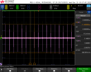
  • I set up probes across the sense resistor and did a difference operation. There are a lot of transients, but the waveform did not change substantially as I changed the load. I've attached the screenshot.

    I also made another very peculiar observation. I was able to get the load up to 7.5 A, but only when I was probing the gate of the FET. Similarly, I was able to jump from 0 A to 7.5 A, but only when I was probing the gate of the FET. What is your take on this?

  • The current limit and RT small-signal components should be directly at the IC pins, no extra spacing. There is switching noise coupling into the current limit circuit based on your waveform. You could try a cap directly at the pins to filter that out (and maybe a series resistor from the shunt to ISEN if needed).

    Also note that SW node copper should be relatively small as this is a radiating surface. Also, the gate drive traces should be wider, 20-30 mils. Take a look at the layout guidelines in the LM5145 datasheet for more detail on buck regulator layout.

    --

    Tim

  • Hi Tim,

    The Rt and Radj resistors are close to the IC. There is a 1 nF cap on the ADJ pin. I could easily put a cap in parallel with Rt, say 100 nF? The SW node copper is fairly large. When I respin the boards, I'll implement those changes. The gate drive trace is only 8 mil, so I'll make it larger. I take it that's why the design worked when I was probing it with an oscilloscope.

    I'll start with a cap at Rt and get back to you.

    Thank you!

  • So I put a 100 nF capacitor in parallel with Rt and I was able to get up to 7.2 A, and I was able to load it from 0 A to 6.5 A without issue. I gave my self ample wiggle room because are a lot of unknowns about this project (believe it or not, it's equipment for vaccine production), but by my calculations (again, a lot of unknowns), we should only need up to 41.6 V and 6.3 A. I'll validate it with my existing prototype. Thanks for your help!

  • Peculiarly, now it seems to only work at Vout max. At any voltage less than that, it cannot regulate at even a small 100 mA load, unless I'm probing the gate. It seems as thought the narrow gate trace is the primary problem. I'm almost wondering if I should bounce it to the bottom layer. What do you think?

  • Also, because I like understanding things (and you seem to know things), and I'd like to explain this to my team tomorrow, why does the gate trace benefit from being wider, and what did probing the gate trace do?

  • Hi Alexander,

    Narrow gate traces increase the gate loop parasitic inductance - hence the recommendation for wider traces, particularly as the gate drive can have high instantaneous current during the switching transitions.

    --

    Tim

  • The small-signal components are too far from the IC - they should all be directly at the applicable IC pins. 100nF might be too much for the RT pin - try 100pF instead or, even better, relocate the resistor closer to the IC.

    Send on a completed quickstart file for review.

  • Hi Tim,

    Something went awry and I spent two days hunting down what turned out to be a cold solder. I added a 220 pF capacitor between RT and gnd (I didn't have 100 pF), and it didn't make any difference. I also had one of our technicians solder a wire between the gate of the FET and pin 6. It's not ideal, but it should reduce the inductance. This also did not make a difference. I also replaced C3 with a 8.2 nF cap, and R10 with a 18.2 kO resistor. This actually helped somewhat. So here is where things stand now:

    1) Load regulation isn't fantastic. Vout climbs with the load. At mid-load, Vout can be as much as 10% higher than at no load. I'm guessing this has to do with noise at FB. I didn't think that this would be a problem for our application, but I ran it with our giant LED array, and it is not finding a stable operating point.

    2) Current limiting is peculiar. If I probe the gate with an oscilloscope probe, it works perfectly. If I don't, it's better than it was originally, but not much better than before I operated on the board.

    I made some changes to the next revision of the PCB layout:

    1) Wider gate traces

    2) Added footprints for caps to ground from RT and ADJ.

    3) Added a footprint in series between ISEN and the low side of the current sense resistor.

    4) Removed power planes from beneath the digital circuitry, instead connecting them with a trace.

    5) Changed the input and output caps to ceramic.

    6) Increased the value of the inductor

    Some questions:

    1) I popped the gate trace onto the bottom layer. I know vias increase inductance. Will this be a problem?

    2) Do you think a choke between Vin and Rt, Radj, and Cadj may help?

    3) Do you think a choke between Vout and Rfb may help?

    4) Might a small bypass capacitor at FB be in order? There is still a lot of high frequency noise there.

    5) Why does the oscilloscope probe at the gate help the current limiting? Electrically, what does it do?

    6) Why do you suspect the voltage regulation is as poor as it is?

    Thank you, and happy holidays!

  • Hi Alexander,

    Here are some answers to your questions:

    1) I popped the gate trace onto the bottom layer. I know vias increase inductance. Will this be a problem? No problem, just keep the gate-source lines short and tight.

    2) Do you think a choke between Vin and Rt, Radj, and Cadj may help? No. Just keep these very close to the IC. Refer to the EVM layout as well.

    3) Do you think a choke between Vout and Rfb may help? No, this needs to be a clean resistor divider. Place the compts right at the FB pin to create a very short FB trace.

    4) Might a small bypass capacitor at FB be in order? There is still a lot of high frequency noise there. Clean up the output with ceramic caps and this should also improve.

    5) Why does the oscilloscope probe at the gate help the current limiting? Electrically, what does it do? Probing the gate should not affect anything (the probe capacitance is much lower than the gate capacitance). I suspect the probe is affect the nearby radiating fields coupling into your circuit.

    6) Why do you suspect the voltage regulation is as poor as it is? Check the ripple amplitude and noise. Vout is typically higher than the output setpoint at no load as the COT architecture regulates at the valley of the ripple voltage (switching occurs when FB decays to the reference voltage).

  • Hi Tim,

    I respun the prototypes, making the changes I outlined here. I was really extremely careful. All the parts are as close to the IC as possible, and I even create a separate analog ground plane, but I was still having exactly problem...until I added some capacitance at FB.

    With no capacitance at FB, I was only able to get to 4.5 A without running into problems. If I put a 100 nF at FB, I could get to 6.5 A before it stopped working. With 200 nF (two 100 nF capacitors in parallel), I got to 8.5 A, and with 300 nF, I broke 10 A.

  • Thanks, Alex, for the update.