Hi team,
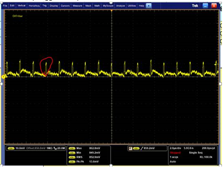
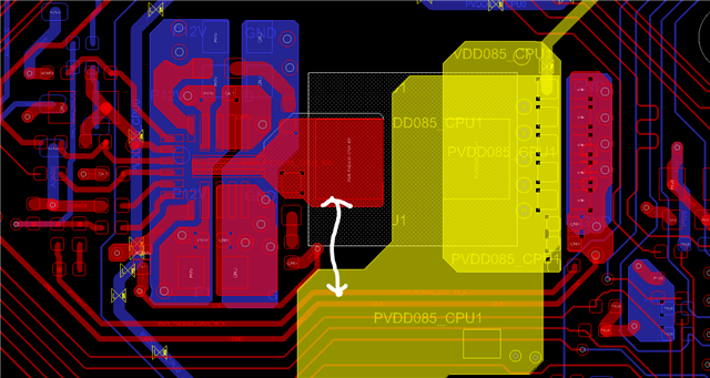
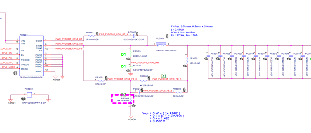
do you think this spike is because FB is too close to SW?
or other causes?
This thread has been locked.
If you have a related question, please click the "Ask a related question" button in the top right corner. The newly created question will be automatically linked to this question.
Hi team,
do you think this spike is because FB is too close to SW?
or other causes?


Hi Fred,
I think the spike may not the true Vout waveform but may be influenced by the probe loop.
You can try to use the pig tail on the scope probe and directly test the both sides of a output capacitor.
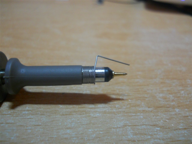
Please let me know if the spike still reserves.
Hi Athos,
we'll check, however I think differently.
since they use 6 TPS568215, only these two have this spike.
so I think their measurement method is the same.
for example this 0.75V doesn't have spike.
Hi Fred,
Just to confirm, is this waveform above the voltage of Vout or FB?
If it's output voltage, I don't think the spike is related to the layout.
FB too close to SW may influence the loop but not the output ripple.
Please let our customer test the SW waveform in the meantime if possible.
Thank you!
Hi Athos,
you're right.
the SW pulse is aligned with the spike in Vout,
is this the inductor materiel problem that cause EMI?
how can we fix this, thanks
Hi Fred,
I think we should firstly ensure the method of measurement is correct to confirm the spike is truly output voltage or injected by the probe.
Do not test GND at a remote point.
Just change some pairs of test points using the pig tail on the scope probe as the above picture, such as directly test the both sides of a output capacitor or test point close to the inductor.
Remember not to test SW voltage in the meantime to avoid the coupling from the probe.
If the spike still remains, please show me the result and let's see if there're some risks of layout.
Hi Fred,
they used pig tail on the scope probe and directly test the both sides of a output capacitor.
but they tested SW at the same time,
I'll tell them to remove it and see if this helps, thanks
would you help explain why probe SW at the same time would couple the SW noise?
Hi Fred,
Thank you for your quick feedback.
You can also advise our customer to change another capacitor and try again to see if the spike is the same.
The probe is sharing the same GND and SW voltage is much larger than the output ripple, so probing SW at the same time may couple some SW noise from GND.
If the duty is low, the phenomenon is more obvious but it's not the true output ripple.
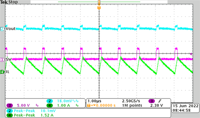
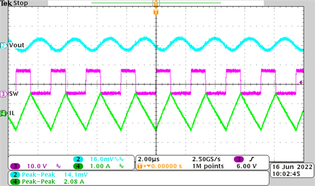
Hi Athos,
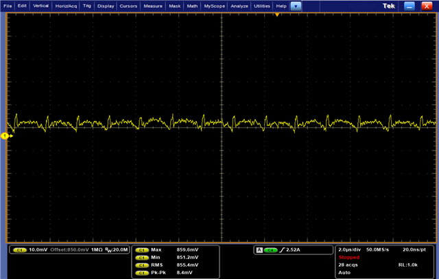
update more waveform,
this time they doesn't probe SW but only Vout (pig tail),
one at DC/DC side, the other at load chip side.
as you can see there's still a small spike there,
what could be the last potential cause? ESR? ESL?
.
.
.
DC/DC side:
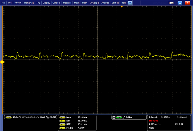
CPU side:
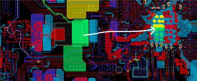
the green is the power rail, you can see the distance between power and CPU side.
Hi Fred,
Thank you for your update.
As you can see, the spike is smaller than before.
The main cause is SW noise coupling, one part is from the probe GND and the other part is from the space coupling on the PCB.
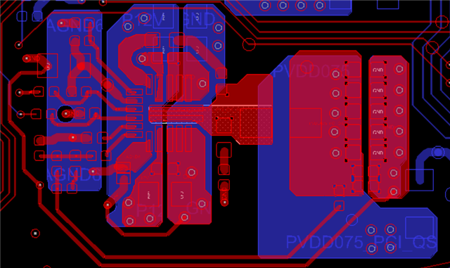
If there're some output capacitors on the bottom layer of the PCB(opposite the inductor), you can try to test Vout there to avoid space coupling.
Also we can put a small PCB/metal board between the inductor and the test point to reduce the space coupling.
And finally, if the ESL of the output capacitors is much larger, the spike will also remain, and different with the above coupling, that's the real output voltage spike. But commonly the ESL will not be so much large to cause the spike.
Hi Athos,
what is space coupling, would you elaborate the detail for me ?
and why bottom side would avoid this?
Hi Fred,
The space coupling here still means the SW noise would influence the probe, from space but not from the wire.
We know the noise is from SW area and if the test point is not on the same layer with the inductor, the noise will not influence the probe so much.
Please let me know if you have further questions.
Hi Athos,
by spacing, you mean EMI?
since they don't probe SW now, so the noise come from electromagnetive wave pick up?
is that what you mean?
Hi Fred,
Yes, it's radiated emissions of EMI from space.
It will also influence the probe result though we use the pig tail.
got it,
looks like the loop of probe has pickup the noise,
will update you after they test on the other side of the board, thanks
Hi Athos,
turns out that the switching noise is "not that obvious" now at bottom side, but the voltage ripple level is still about same as the top layer.
they try to add 22uF MLCC but doesn't help, do you think we should add 0.1uF instead to further minimize ripple?
Hi Fred,
The ripple is ~8mV and I think it's not easy to minimize.
Also it's not so easy to measure the accurate real ripple under 10mV.
Adding 0.1uF capacitor is to minimize the high frequency ripple but may not be suitable for this case.
I think the most effective way is that we can try to use 1.2MHz Fsw to minimize the ripple.
If the frequency can't be changed, usually we can reduce the inductance or add output capacitor to minimize the ripple if it's indeed required.
You can also advise our customer to use a 2nd stage LC filter after the output to realize a smaller ripple.
Hi Athos,
you said add extra output cap would help, but they try extra 22uF but on much change.
may I know why?
do you think is because 8mV is dominated by noise instead of true ripple , so the improvement is not obvious?
Hi Fred,
I can't see the whole schematic but I find there's already 7*22uF output capacitors.
The ripple is basically decided by the below equation.

You can see add one 22uF capacitor may not influence the ripple so much.