


Other Parts Discussed in Thread: UCC28070
Hi All.
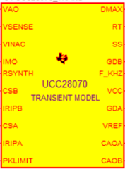
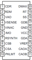
What does IRIPA, IRIPB and F_KHZ pin in UCC28070 Transient model represent?
Original question:

TINA/Spice/OPA322: How to use "Import TINA Libraries and Designs" feature in TINA-TI v9?
Hi All.
What does IRIPA, IRIPB and F_KHZ pin in UCC28070 Transient model represent?
