Hi,
I was resolving problem with noise on AVDD with Patrick Yao here:
Here are the results after PCB modifications:
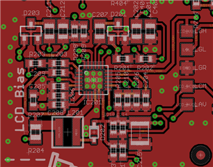
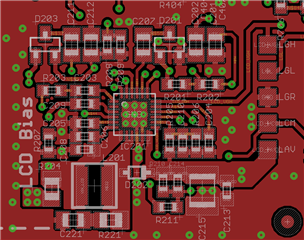
1) enhanced connection in coil and output, shifted diode and capacitors positions, added snuber (C221+R221), Left OLD design, Right: NEW design
2) Waveform without snubber (Measured SW-GND)
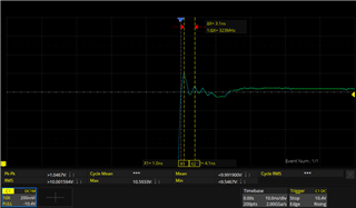
3) Waveform with half snubber, 270p+0R (Measured SW-GND)
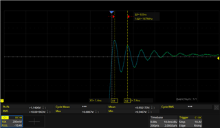
4) Waveform with full snubber, 270p+5R1 (Measured SW-GND)
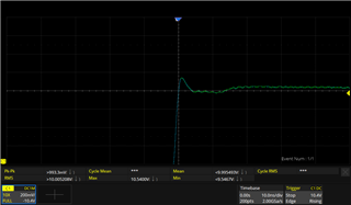
5) and 6) Waveform, Left: Measured AVDD on testpoints (LAV and LGD), Right: Measured on C213:
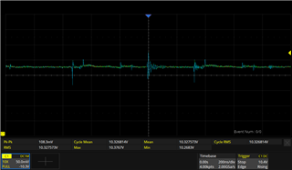
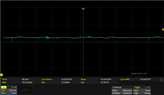
7) comparision of waveforms measured AVDD on testpoíints: Left: OLD design (no snubber), Right: NEW design (with snubber)
- timebase is not same... left 500 ns/div, right 200 ns/div
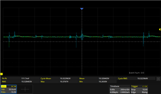

8) comparision of waveforms measured AVDD on output capacitor (left C215, right C213): Left: OLD design (no snubber), Right: NEW design (with snubber)
- timebase is not same... left 500 ns/div, right 200 ns/div
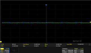

The ringing on the coil is suppressed, but the noise on the testpoints are still there, although a bit lower (117 vs 108 mVp-p on testpoints and 48 vs 38 mVp-p on output capacitor).
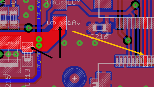
Here is highlighted AVDD signal (PCB is 4-layer, but in image is visible only TOP+BOTTOM layers):
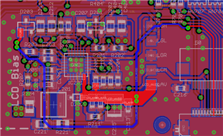
Do you see a problem with tracing AVDD wire or any other problem that could generate noise on AVDD?
Thanks!


