This thread has been locked.

If you have a related question, please click the "Ask a related question" button in the top right corner. The newly created question will be automatically linked to this question.

LM5116: Converter Failing to Start Under Load - Low VCCX/VCC

Part Number: LM5116

We recently received a new batch of boards with a 24V buck converter that was failing production testing. The production test turns on a 4Ω resistive load, enables the 24V converter, and then tests the 24V rail. 

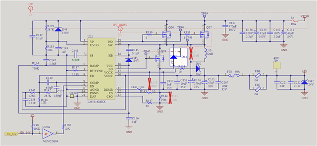
This converter uses the LM5116 with the specifications:

VIN: 36-85V

Vout: 24V

Iout(max): 8A

fsw: 200kHz

Tss: 50ms

High-side Switches: SIR632DP-T1-RE3

Low-side Switch: BSC077N12NS3 G

This converter has worked fine in the past (albeit, not optimally); however, these boards do have a component change. The converter schematic is shown below. D44 (NTS10120MFS), in parallel with the low-side synchronous switch, was changed to a new component with a slightly higher forward voltage drop: +0.2V (MBR15200DJF). Given this diode is not necessary, I am skeptical it is the cause of the problem. 

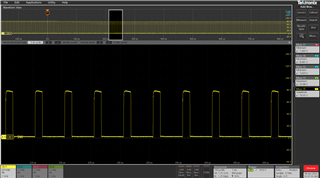
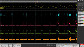
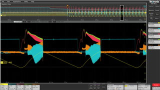
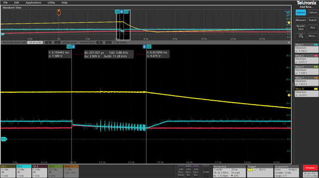
During testing, I found that the converter was hiccupping soon after the VCC voltage source was changed from the internal 7.4V LDO to VCCX.  At this point, VCC drops down to ~5V, and then decays more slowly over the next few switching cycles to 4.7V. This was only experienced when starting under a load above ~4.5A. The next image shows VCC falling during a hiccup cycle. Yellow is Vout, blue is VCC, and red is VCCX.

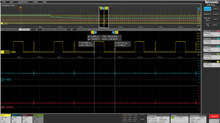
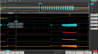
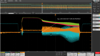
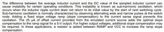
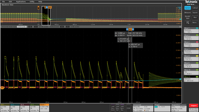
During this time, the Vgs of both low- and high-side switches also drop, causing poor enhancement of the FETs. In the image below, VCC is blue, high-side Vgs is orange, and the yellow and green signals are HO and SW, respectively. Please note, this poor turn-on is also seen on boards that start up under load and pass production testing. Furthermore, if a converter is able to ride out this period, VCCX increases, and the gates begin to operate normally. The margin between starting completely and not is clearly small.

I'm making this post slightly prematurely as I'm about to perform some more tests; however, it would be beneficial to have answers to the following questions:

1.) Would a different parallel low-side diode cause significant change to the switch node during this period that would explain why these boards do not function as well? I both removed the diode and replaced it with the old one and got the same result in each case. Does this then point to another change?

2.) If the switches are not turning on completely, what is actually causing the converter to turn off? We see large current spikes at this time (measured using the differential voltage of CS and CSG), but these are short in duration, and I don't think are likely to trip the OCP. Is the converter then just experiencing a VCC under-voltage fault? 

3.) If we add additional capacitance on VCC/VCCX to allow VCC to remain higher for longer, will this allow the converter to get through the initial start-up?

4.) I calculated Igc as 14mA. If I were to ground VCCX and remove its function, would we experience excessive heating or poor performance? The datasheet recommends <15mA. 

5.) Could tolerance stack-up in components (VCC/VCCX capacitors, bootstrap diode, LM5116 VCC undervoltage) just happen to be enough to impact the converter given its small VCC margin?

The design of this converter is being updated in a new revision of the board, but we have a stock of the current revision that we need to use. We have already noted a number of sub-optimal elements that will be addressed in the new design. What I am concerned with at this point is what is causing this latest batch of boards to not function correctly, when others did previously.

Any help would be welcome!

  • Hi,

    This thread has been received and I will get an appropriate apps contact to support your question. 

    Regards,

    Jimmy 

  • Hi Logan,

    What's the FET part number? It's likely that the FET Miller plateau is close to 5V, so the VCC swing low during transition to VCCX results in inadequate turn-on of the FETs. The Miller plateau increases at cold, which is worst case for this potential issue.

    Regards,

    Tim

  • Hi Tim,

    The FET in question is a SIR632DP-T1-RE3. There are two of them on the high side. Based on the Vgs-Qg graph, it is approximately 4.5V. 


    I did more testing after making the original post, including removing the VCCX function entirely. The converter will then start properly under load. This is an option moving forward, albeit with the increased power consumption not being less than ideal. 

    I still do not understand why the new diode causes worse performance in the converter. I took an old board with a working converter and replaced the low-side diode with the new part, and it made a visible change in the switching waveform. My assumption is the cycle-by-cycle over-current protection is kicking in. 

    Before:


    After: 


    Every other switching cycle, the gate is turned off prematurely, coinciding with a spike on the UVLO and VCC. This did not stop the converter from starting up, however. After approximately the same amount of time, VCCX would continue to increase, the FETs would fully enhance, and the converter would turn on completely. 

    Do you have a suggestion as to why this new diode might be causing this to happen? I'll readily accept the margins of the signals in this converter are very small, but I'd like to understand why changing this diode causes a significant enough change to cause such a problem. It seems like the previous build of boards will continue to operate with the new part, so it's possible the tolerances of various other components used in this latest batch add up to create a "perfect storm". 

    For reference again, these are the two diodes:


    Original: NTS10120MFS

    Replacement: MBR15200DJF

    Thanks again for your help,

    Logan

  • Hi Logan 

    I guess the difference is caused because the junction capacitance of MBR15200 is greater than NTS10120's. If any chance, please monitor Vgh_high,  Vgs_low and inductor current together. 

    - Eric Lee

  • Hi Eric,

    The waveforms below are from a non-functioning converter with the new MBR15200 diode, loaded to 6A. CH1, CH2, CH3, and CH4, are the inductor current, Vgs_Low, switch node voltage, and HO, respectively. The Math function is Vgs_High. 

    At t=-26µs, every-other high-side gate ON pulse begins to decrease. At t=29µs, the high-side switch does not turn off properly. The switch node voltage appears to decay faster than 150ns in the previous switching cycle.

    I reduced the load to 2.67A and repeated the measurements. Here, the converter will start up successfully, but the switches exhibit the same features. 

    At this load, the inductor current becomes negative during the switching cycle. 

    Reading the datasheet, it mentions wide and narrow pulses at the switch node being an indicator of sub-harmonic oscillation. Can this be a possible explanation for the alternating pulse widths seen just before the converter reaches this point?

    Thanks again for your help,

    Logan

  • Hi Logan 

    The sub-harmonic oscillation happens when the duty cycle is less than ~ 50% and the amount of slope compensation is not enough. I don't think you are seeing the sub-harmonic oscillation because the input voltage is ~ 80V, but if you are concerning about the sub-harmonic oscillation, you can simply check it by reducing the Rramp resistor value. Also, please double check your Rramp and Cramp values using the Quick Start calculator https://www.ti.com/lit/zip/snvu051 

    -Eric Lee

  • Hello again Eric, 

    I checked the values of the compensation components, and they seem satisfactory; however, I do have a development on a different front. 

    Based on the same quickstart sheet, I found that the bootstrap capacitor is low. The value I calculated was 0.26µF whereas the current capacitor is only 0.1µF. The datasheet recommends a 1µF capacitor, 10x what is currently in the design. Using this document (Bootstrap Circuitry Selection for Half Bridge Configurations), I manually calculated the minimum bootstrap capacitor value, with a similar result of 0.22µF. 

    After finding this, I replaced the bootstrap capacitor with a 0.33µF capacitor and it successfully started at the 6A load. The switching waveforms are still not pretty, but it did start consistently. Bumping the load up to 8A stopped it from starting again, though based on the recommendation in the datasheet, it looks like I should try increasing this to 1µF. 

    The same document linked above recommends that the VCC bypass capacitor be 10x the bootstrap capacitance. If the bootstrap is too low, this value may also be insufficient to supply the needed charge. Once again, I've found a feature of this design that is sub-optimal, but why it was exposed by this new diode is not something I have been able to say I understand definitively. 

    Q: In your experience, would a change in the junction capacitance of the diode cause a noticeable change in the performance of the bootstrap capacitor/charge pump? Based on the plots in both datasheets, I believe when reverse-biased at 85V, the new diode (MBR15200) actually has a smaller capacitance. I can only infer this is the case, as the MBR plot only goes to 40V. The difference between the two is very small, on the order of 10s of picofarads. 

    If you can please provide me with any final thoughts, I'll close this topic. I've identified a number of deficiencies in the design (switch turn-on, VCCX instability, bootstrap charge) that will be solved in the next board update, and the reason why these latest boards do not work compared to the previous batch may be chalked up to poor margins and tolerance stackup of the various components. 

    Cheers!

    Logan

  • Hi Logan 

    V(Chb) is proportional with V(VCC)-V(SW)-V(Dhb) during dead-times. Which means the negative spike at the SW node affects the Chb voltage. Usually, the amount of negative spike is proportional with the forward voltage drop of the low side MOSFET body diode (or the external diode in parallel with the low-side MOSFET). In your case, the more negative spike is the better  because you have to make V(Chb) greater than the miller plateau voltage. 

    'Cvcc > 10 x Chb' is recommended. Also, it is recommended to make Chb > 10 Cg 

    In your case, the bigger Chb is the better because you have to keep V(Chb) greater than the miller plateau voltage during the the high-side MOSFET turn-on time.  

    - Eric Lee

  • That makes sense. Thanks again Eric. I appreciate the help.