This thread has been locked.

If you have a related question, please click the "Ask a related question" button in the top right corner. The newly created question will be automatically linked to this question.

offline Controller IC for forward converter

Other Parts Discussed in Thread: UCC2894, UCC28C53, UCC2897A, TL431, TLV431

Hi Sir,

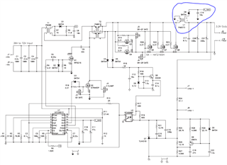
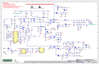
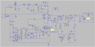
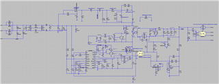
I would like to design a offline power supply using forward converter topology. 

The specifications are as follows 

Input voltage: 50V to 200V

Output voltage: 5V or 15V or 24V

Power rating: 50W or 100W or 300W

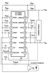
Please suggest suitable controller IC for the above requirement. 

Thanks in advance for your suggestions. 

Thanks and Regards

Umamaheswararao

  • Hi,

    You may consider the below:

    UCC2894, UCC28C53, UCC2808

    If you have some special feature requirements, please provide so we can adjust or refine our recommendations.

  • Hi HH,

    Thank you for your reply. 

    I just gone through the overview of datasheets of suggested ICs. I have observed that the input minimum 85V (universal input) is required for UCC2894, UCC28C53 as per datasheets. Can you Please send the any design documents for Input voltage range 50V to 200V DC. 

    Thank you

    Umamaheswararao Vuyyuru

  • Hi HH, 

    Thank you for your suggestion. I am going through IC UCC2894 for my design. 

    Regards

    Umamaheswaraaro

  • Hi Sir, 

    Can you please tell the difference between UCC2894 and UCC2897A

  • Hi,

    UCC2897A needs p channel FET for low side clamping but p channel FET over 200V not easy to get or with high cost.

    UCC2894 needs n channel FET for high side clamping but many options for n channel FET and with lower cost.

    Your design with up to 200Vin so UCC2894 is recommended.

  • Hi, 

    Thank you for your reply. Can please explain the advantages and need of "BIAS
    WINDING" in the UCC2897A and please suggest me if same is required for UCC2894. 

    Thanks and Regards

    Umamaheswararo

  • Hi,

    The bias winding design is same.

  • Hi Sir,

    As per the datasheet of UCC2894, Vdd supply is taken from the output side filter inductor, the screenshot is give below for the quick reference. 

    Can we take the bias power supply from the auxiliary winding of the transformer? Please suggest. 

    Thanks and Regards

    Umamaheswararao 

  • Hi,

    Yes, you can design the bias from the transformer auxiliary winding or from the output inductor.

  • Hi,

    Thank you for quick reply. Can you please tell me the difference between two and which is best. 

    Thank you

    Umamaheswararao

  • Hi,

    The reference with the inductor is due to its convenience. There is not difference on the operation.

  • Hi, 

    Thank you for the reply. Can you suggest how to select the exact value of clamping capacitor for flyback and forward. As we are planning to design both the converters using UCC2894. please share if any design files are available for both the topologies. 

    Thank you

  • Hi,

    You can refer to the below application note for your design. The clamping capacitor value typically between 33nF and 100nF, requiring tuning up. You can start with 33nF.

    Understanding and Designing an Active Clamp Current Mode Controlled Converter (Rev. A).

  • Hi Thank you for your answer. I am calculating the RF, Rslope, Rsense resistors. Can I take below document as a reference 

    https://www.ti.com/lit/an/slua584a/slua584a.pdf?ts=1673935788655&ref_url=https%253A%252F%252Fwww.google.com%252F

    Please suggest. 

    What will be the current at RSLOPE pin. If I take 30uA, then my Rslope will be (1.27V/30uA) = 42.3kR. Is this correct?

    Please suggest

    Thank you

    Uma

  • Hi Sir, 

    I am waiting for the reply. 

    Thank you

  • Hi,

    I suggest you take reference of what I provided to design current sense and slope compensation. The application note is not for UCC2897A so you may not get correct detail although you can take it as reference.

    Rslope voltage is 2V instead of 1.27V. So for 30uA, Rslope = 2V/30uA = 66.7k.

  • Hi Sir,

    Thank you for your reply.In page number 36, 

    As per data sheet, the minimum reverence voltage of TL431 is 2.45.

    Please explain, 

    1. How Vref and Vsc is 1.25V?

    2. The required output voltage is 15V, if I connect the optocoupler to Vout through R_OPTO, can I take V_opto as 15V for the R_opto calculation?

    Thank you

    Umamaheswararao

  • Hi,

    The application note uses TLV431, and if you read the associated content, the note mentions a ref of TLV431 is 1.24V.

    Vopto is 15V if you connect it to 15V.

  • Hi Sir,

    Thank you for your reply, If I consider Vopto=15V, the Ropto is 3.162k

    the Gopto is -ve in db

    If gopt is -ve, is this okay for control design. 

    Please suggest. as for the document, Gopto is +ve, give below for your quick reference

    Thanks in advance your support 

    Thank you

    Umamaheswararao

  • Hi,

    You need to get a +ve.

    There are several ways to do this.

    One is to have a Zener and reduce from 15V to a lower say 5 to 10V, then Vopto  is lower, so the resistor Ropto value will be lower. This should be easiest way.

    Second, is to use TL431 instead of TLV431, so the reference 2.5V instead of 1.24V since your Vout is higher so you can use TL431.

    Third is to find an optocoupler with CTR higher than 2 so to help +ve.

     Among these, if you use an Zener, then you will get +ve quite right away.

  • Hi Sir,

    Thank you for your reply. I will the zenor and TL431 to make the positive gain. 

    As per my understanding from above circuit, R13 is current limiting resistor for the zener,  Ropto is R15. What is R14?

    If Vopto = 9.5 (minimum voltage of Zener)

    VF =  1.3V

    Vsc (TL431 minimum) = 2.45V

    I_TL431 = 1.3mA

    R_opto/R15 = 1459 Ohms  (Please confirm is this correct?)

    This value is different in the above referred circuit. If I consider, 3.6mA then R15 is 499 Ohms. If I consider 3.6mA based on CTR ratio, the refelected current on the transistor side of the optocoupler is more. 

    As per the controller IC (UCC2894D), V_ref max is 2mA

    In the application note, R_ref is calculated based on maximum current drawn from the Vref pin. For quick reference same is given below

    From the above screenshot, I am not understanding the following line "The minimum voltage on the feedback pin to get output pulses is defined by the Current Sense Level Shift voltage times the resistor ratio within the device which yields (0.48V × 5) 2.4V."

    For UCC2894D, the CS pin voltage is 1.27v, from this if I calculate the minimum voltage at the feedback pin to get the output pulses is 6.35 (1.27*5) 

    V_ref is 5V

    V_fb_max is 6.35

    I_ref_min is -Ve

    Is ths corrrect?

    Please suggest how to calculate the R_ref for UCC2894D as well. 

    Thanks in advance for your support. 

    Regards

    Umamaheswararao

  • Hi,

    R14 is to set up a bias to opto coupler so opto coupler is not in fully cut off.

    R_ref should be 2k and always like this based on many designs. other values cannot make the IC work properly.

    UCC2894 FB voltage range to have switching pulses is between 1.25V and 4.5V so different from UCC2897A.

    Note (0.48V x 5) = 2.4V, so the equal symbol missing.

    I_TL431 usually consider about 1 mA in a design as best option from many designs. You adjust other parameter values to achieve proper design but keep the above as default and usually no need to redesign as these proved close to best.

  • Hi Sir,

    Thank you for reply.

    1. If take R_ref is 2k, waht will be the minimum voltage at FB pin? What is resistor ratio for UCC2894D (it is mentioned that 5 is the resistor ratio is 5 in UCC2897A application note)

    2. if I consider I_TL431 is 1mA, R_opto is 1.897k, Please confirm the same and Can I take R14 and R15 same?

    3.  "You adjust other parameter values to achieve proper design but keep the above as default and usually no need to redesign as these proved close to best."  from this line, as per my understanding, i have to redesign the R14, R15, R_ref and the remaining all parameters can be same, please confirm. 

    Regards

    Umamaheswararao

  • Hi,

    1. R_ref is connected to VREF (=5V), so to make FB = 1.25V, the I_ref = (5V-1.25V) / 2k = 1.875mA, so you need to design your opto able to sink 1.875mA, or roughly 2mA, then FB can reach 1.25V. UCC2894 structure is slightly different and please refer to page 6 diagram of its datasheet.

    2. R14 should be about 0.5 to 1k for most of the opto coupler. R15 is your Ropto which value needs to design and follow the application note.

    3. R14 is about 0.5 to 1k, you can keep 499-ohm, the remaining needs to design to check if they are ok, for example, +ve is required and if you get -ve you have to adjust your design to achieve +ve.

  • Hi Sir,

    Thank you for your suggestions. I will consider the same for my design. If I have any question, I will contact you. 

    Regards

    Umamaheswararao

  • Hi Sir,

    As you suggested, UCC2897A can be used only for p channel FET. But, as per the below document, UCC2897A can be used for high side clamping with N channel FET. Please confirm the same

    Please suggest the best one. 

    Thanks and Regards

    Umamaheswararao

  • Hi,

    If you add external inverting driving transformer, ucc2897a is ok to use for n mosfet.

    in general, for vin > 100v, we recommend ucc2894 with n fet clamping.

    some designs like use ucc2897a with external driving transformer with n fet because the designs want to go with lower cs threshold.

    besides, ucc2897a VIN pin cannot be used when vin > 100v.

    in your design, I still recommend ucc2894, but if you want you can use ucc2897a if you think it’s cs threshold is better, which usually reduces power losses but more likely affected by noise in high vin applications.

  • Hi Sir,

    Thank you for your reply. As per my understanding, external inverting driving transformer is not required for UCC2894 for high side N-mosfet clamping. Am I correct please suggest. My draft schematic is given below please suggest If I missed any thing. 

    Once schematic if finalized, I will update the ratings of each components. 

    Thanks in advance for your inputs. 

    Regards

    Umamaheswararao

  • Hi,

    ucc2894 requires a driving transformer for high side clamping FET. So you need to add that transformer into your circuit.

  • Hi sir,

    Please check the modified circuit as per your suggestion. 

    Please suggest if required any modifications in

    1. Bias circuit

    2. Driver circuit 

    3. Compensator 

    4. EMI filter

    Thank you

    Umamaheswararao

  • Hi,

    As this is to review the schematics, it requires time. I will reply to you in about one week.

  • Hi,

    1) Note 12V Bias needs to reach 13.2V in order to start up UCC2894.

    2) 

    3) 

    4) Do you think you also need to have a differential choke in your EMI filter?

  • Hi Sir,

    1) Note 12V Bias needs to reach 13.2V in order to start up UCC2894.

    Thank you for the suggestion, I will change the Zennor diode (witch is connected to the series regulator directly connected to the Vdc input) to 13.2V to get the initial voltage. 

    4) Do you think you also need to have a differential choke in your EMI filter?

    I dont have any idea about EMI filter, Please suggest. 

    Please suggest if any further modifications are required. 

    Thank you 

    Umamaheswararao

  • Hi,

    I suggest to add a place holder for differential mode choke. In most cases, a differential mode choke is needed. In the best case, you can just leave that place holder unpopulated.

    If you have no idea how to design EMI filter, I would suggest you first to look into anybody within your team or group with such expertise. EMI is kind of tricky and usually not easy to handle if without any experience or without any expertise nearby when you want to pass EMI test.

    There are many literatures on EMI. So you may need to review these to gain knowledge.

  • Hi,

    Thank you for the reply. Now, UCC2894D is available with me. I want to know the working status of IC UCC2894D before soldering in the main board. What are parameters I have check. Please suggest. 

    Thank You

    Umamaheswararao

  • Hi,

    To check, you need to add all UCC2894 needed external components on its each pins based on your design. Then bring its VDD above 13.2V, you should see its VREF becomes 5V, SS becomes from 0 to 5V. FB needs to be > 1.25V, (say set up to be 2V), LineUV > 1.3V, LinOV < 1.2V, then you should see OUT and AUX pulses, the switching frequency should be based on your designed value. If you can see OUT and AUX pulses ok and fsw is your designed value, the IC is working.

    If you want, you can find a way to pull up CS > 0.75V to check OUT and AUX pulses stop.

    Also, pull down SS, will stop OUT AUX pulses.

    Please read through the datasheet to check anything else - you would need to familiar with the datasheet in order to use this device.

  • Hi,

    Thank you for the reply. I have connected all the external components as per the datasheet

    for the testing, following values are used 

    RDEL = 10k, RTON = 71k, RTOFF = 150k, CVref = 0.1uF, CF =  0.1uF (no RF connection), Rslope = 47k, Css = 0.1uF, CHF = 0.22uF, Vin =59V, RIN1 = 141k, RIN2 = 3.9k, RIN3 = 141k, RIN4 = 2.7k, Rvref = 2k, 

    Vdd is given using external power supply (set to 13.2V at the starting and thereafter maintained to 12V)

    Vref alos given using external power supply (2.2V)

    Observations:

    1. At Rslope pin, 196kHz waveform is generated  (pin number 8)

    2. Vref = 5.1V generated  (pin number 4)

    3. 0.95V is obtained at SS/SD pin (pin number 10)

    4. LineUV= 1.31V generated  (pin number 15)

    5. LineOV= 0.95V generated  (pin number 16)

    6. No pulses at Pin 12 and 13 (OUT and AUX)

    As you mentioned SS pin voltage becomes 0 to 5V, but it is not happing. Please suggest if any modifications are required in the circuit or components design. 

    Thank you

    Umamaheswararao 

  • Hi,

    Please provide the waveform of CS, SS, FB and OUT.

    Also increase Vdd to be 14V for the test.

  • Hi,

    Sorry for the late reply. As per your suggestion, I have applied 14V at Vdd and the corresponding waveforms are as follows 

    1. FB and OUT

    2. OUT


    3.Vref and SS/SD

    4. RSLOPE

    5. CS and OUT

    Voltage at SS pin is below 1V and no OUT signal. Please suggest, 

    Thanks in advance for your support.

    Regards

    Umamaheswararao 

  • Hi,

    The SS needs rise up to 5V and stays there to work.

    First check the capacitor value and connection on SS to make sure ok.

    Then capture waveforms SS with the below:

    Vdd, LineUV, LineOV, Vref

    and provide these waveforms for analysis

  • Hi,

    Thank you for your inputs. I have increased the VDD capacitance to 220uF, Now, SS pin charged to 5V and at OUT pin pules are OK and varying duty ration with Vfb.

    Thank you

    Umamaheswararao 

  • Hi Sir,

    Can you please suggest the output Short-circuit protection circuit using UCC2894 IC. 

    Thanks and Regards

    Umamaheswararao

  • Hi,

    You need to specify your OCP or short circuit protection specs.

    UCC2894 has embedded OCP in cycle by cycle current limit, which is also ok for short circuit protection. You need to decide if these ok with you or you need different. If different then external circuit needs to add but then an external design to UCC2894.