This thread has been locked.

If you have a related question, please click the "Ask a related question" button in the top right corner. The newly created question will be automatically linked to this question.

BQ77915: Short Circuit Is Not Working

Part Number: BQ77915
Other Parts Discussed in Thread: BQ76200, BQ76940,

Hi 

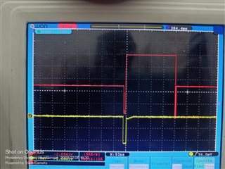
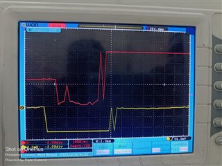
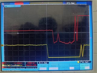
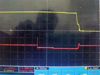
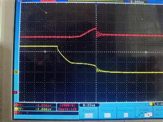
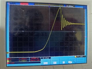
I am Saikat Jana I am working on BMS and Battery Pack Design and for that we are using BQ7791501 as protection IC all the other protection related to the battery pack is working fine (OCD,over temperature, Over Voltage , Under Voltage ) but short circuit is not working. 

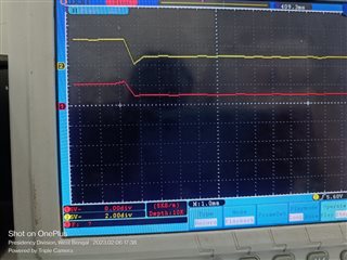
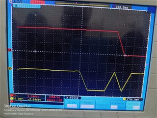
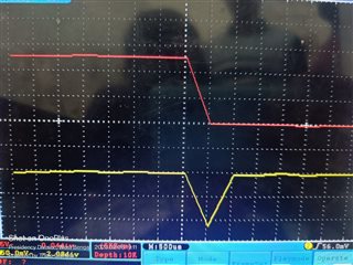
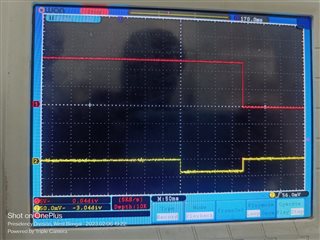
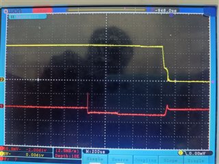
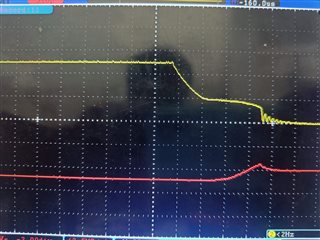
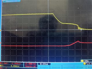
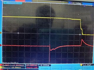
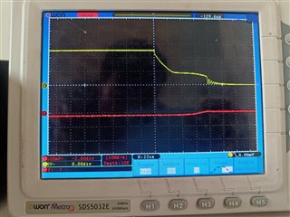
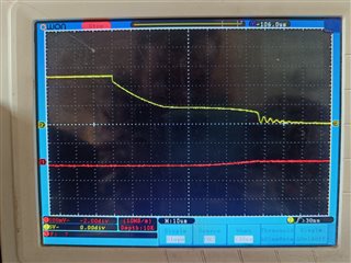
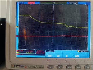
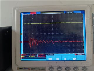
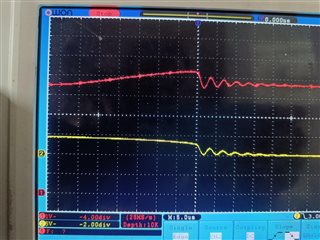
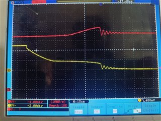
Process for Short Circuit Test - Short Pack+ and Pack- 

Result - Discharging MOSFET get damaged every time 

We need to release our product by February and we already have pre orders for that but without short circuit feature we will not able to release the product. 

Please help us to release the product as early as possible and me know what tech details I need to provide, ckt-15s (3).pdfHY4008B.pdf

Thanks in Advance 

Saikat Jana 

  • Hello Saikat,

    Do you have any waveform of the DSG gate/source during the SCD? Is the CHG FET affected, or just the DSG FET? How is it failing?

    There are different scenarios where the FETs can fail, here is an e2e thread that discusses possible causes: 

    https://e2e.ti.com/support/power-management-group/power-management/f/power-management-forum/1054353/faq-bq769142-mosfet-short-after-short-circuit-test---voltage-now-always-on/3900591#3900591

    One thing I notice from your schematic is that there are no individual gate resistors for each FET. Did the FET provider say it was okay to parallel them without them?

    Typically when paralleling FET it is recommended to add a ferrite bead or a gate resistance (some providers recommend a gate resistance of 10% of the driver load, in this case a ~50-Ohm resistance would be okay). This just ensures there are no parasitic oscillations between the FETs during the turn-off.

    Best Regards,

    Luis Hernandez Salomon

  • Hi 

    Thanks for your reply

    Currently, we don't have any waveform captured during the SCD event. No CHG FET is Not Affected only DSG FET Is Burning and some it Blasting like Bombs. 

    We don't have any recommendations from the manufacturer's end, Whatever you suggest we can test and modify our circuit accordingly.

    Our Battery Pack Capacity for Liion - 14S (51.8V Nominal) 60Ah

    Li-ion Cell Specification - 18650 (3.7V - 2900mAh) 3C Liion-NMC Cell 

    Thanks 

    Saikat

  • Hello Saikat,

    It may be difficult to debug without having a waveform with the SCD event. I would greatly recommend looking into the e2e post I shared for some of the common topics that affect the SCD protections.

    Definitely would recommend to add ~50-Ohm resistor or a ferrite bead at the gate of every single FET in your application. If FET oscillations is the cause for the failure, these would mitigate them and protect the FETs.

    If the turn-off is too fast it is possible for the transients generated to cause issues, which in these cases you may need to slow the turn-off. Inversely, if turn-off is too slow, the FET could burn due to the current flowing when the FET is highly resistive, in which case turn-off needs to be sped up. 

    Having a waveform of the event would be useful. But if not, you can try the things I mentioned above and what the E2E thread I shared mentions (https://e2e.ti.com/support/power-management-group/power-management/f/power-management-forum/1054353/faq-bq769142-mosfet-short-after-short-circuit-test---voltage-now-always-on/3900591#3900591).

    An additional question, are C30/C31 ceramic capacitors? 

    Best Regards,

    Luis Hernandez salomon

  • Hi 

    Thanks for the valuable feedback 

    Please let me know what waveform you want to see Like - SRP and SRN or VGS of the Mosfet or DSG pin Voltage with respect to ground 

    We will capture that and update you

    We have added the 50-Ohm resistor in every MOSFET and we can see SCD is working on the Small battery pack 

    14S(51.8V) 15Ah and SCD threshold is 60A  but when we connect our BMS with a big battery pack 14S(51.8V) 60Ah and SCD threshold - 120A Mosfet burns again 


    Please suggest to us the value for R17 Resistor now we are using 5.1K 

    C30 and C31 are MLCC (Multi-Layer Ceramic Capacitor ) capacitors.

    We have also designed one SMART BMS using BQ7694003 and for that circuit, we need some help on the Charger detection circuit 

    For Smart BMS we are doing High Side switching using bq76200

    Thanks for Your Support 

    Saikat 

  • Hi 

    We also try with a reduced R17 (3.3K) Value but same result 

  • Hello Saikat,

    A waveform showing SRP/SRN with the VGS of the DSG FET would be great. Also show PACK- to Vss in the same image if possible.

    I am glad to hear that adding the 50-Ohm to the gate of the FETs made the smaller pack work. Could you possibly replace R17 with a smaller resistor (maybe 100-Ohm) and see if there's any improvement for the larger pack?

    Regarding your new question about the BQ76940, would you open a new thread with more details on it? We will be able to better support you there.

    Best Regards,

    Luis Hernandez Salomon

  • Hi 

    Thanks for your valuable reply 

    For a better understanding of waveform 

    what do you want the difference between Voltage on SRP and SRN, Waveform between DSG FET VGS with respect to Batt- and PACK- to Vss

    am I correctly understood ??

    Is there any formula to calculate the value of R17 

    Battery Pack Spec -

    Nominal Voltage - 51.8V

    Full Charge Voltage - 58.8

    Battery Type - Li-ion NMC (3C)

    Max Discharge Current - (5C)

    Nominal Capacity - 60A

    Mosfet in parallel - 3/4

    Thanks for your valuable support , we need to resolve the issue by Jan 2023

    Saikat Jana

  • Waiting for your valuable reply

  • Hello Saikat,

    Correct, SRN - SRP would just allow us to see what is the current flowing through the sense resistor. PACK- to Vss or BAT- would be okay and DSG FET gate to bat- or Vss would also be okay.

    There is no formula to calculate the value of R17, as this is very dependent on the end equipment, layout, currents, etc. As every system will have different level of parasitics of short-circuit currents.

    The FAQ I sent earlier lists all possible reasons the FET could become damaged and why it is difficult to choose the right valued resistance.

    Did you attempt to use a smaller R17 resistor to see the result? In the case that the turn-off is too slow, a smaller resistor will allow the FET to turn-off faster. The turn-on/off speed is dependent on the total FET capacitance (the more FETs the longer it will take) and the common gate resistance (R17).

    Best Regards,

    Luis Hernandez Salomon

  • Sure We Will Capture the waveform in a day or two 

    for the short circuit, we are just short the pack- and bat+ 

    We will test and let you know the result of 100 Ohm (R17) by tomorrow 

    Thanks 

    Saikat

  • Ok! Looking forward to it!

    I'll make sure to support you all of this week so that we can hopefully solve this issue by the end of the month.

    Best Regards,

    Luis Hernandez Salomon

  • Hi

    How mutch gates current BQ77915 can provide ??

  • Hi

    As per my understanding, 100ohm is really small 
    can bq77915 DSG pin handle this current ??

    Please Let Us know so that we can start 

    Thanks for your valuable support 

  • Hello Saikat,

    The BQ77915 was not characterized with a specific driver strength. It was characterized with rise/fall times, it also provides resistances when OFF (Typical 10-Ohm for the DSG driver). 

    100-Ohm should be okay with the device. But you can test with 1-kOhm instead of 100-Ohm for now to start. The idea of using a small resistance is that the capacitance of the FETs is slowing the turn-off speed (due to larger RC constant as there are many FETs in parallel), so we use a smaller common gate resistance to decrease the RC constant and turn-off the FETs faster. This is assuming that the FETs are breaking due to slow turn-off speeds.

    The waveform would give us a better idea as to what is going on.

    Best Regards,

    Luis Hernandez Salomon

  • Hi 

    Tested with 1K but still burns more badly than previous 

    This happens very high speed so I am not sure How to capture the waveform 


    Thanks for your valuable support
    Saikat

  • Hello Saikat,

    Did you set a trigger as a falling edge in your oscilloscope? You could put the trigger at the gate-source of the DSG FET. You could adjust the time scale to maybe 20-us or up-to 100-us and see how it looks.

    Without a waveform it is very difficult to know what exactly is going on unfortunately.

    Best Regards,

    Luis Hernandez Salomon

  • Saikat, 

    Since the first battery pack was fixed by adding the individual 50-Ohm resistances. Maybe you can attempt to increase this resistance to a higher value, like 100-Ohm or 200-Ohm.

    Best Regards,

    Luis Hernandez Salomon

  • Hi 

    Sorry for the late response, I did more testing but using both BQ76940 and BQ77915 both failed I have captured the waveforms from BQ76940, and from What I understand there is no Timeing oriented problem and also SCD works at 67A Current, and when I increase the current threshold to 90A it failed again. Please have a look at Waveform 

    Yellow is the gate voltage 
    Red is the Pack Voltage

  • Each gate already has 120R ferrite bead

  • We also captured the waveform for BQ7791501. Controlled (Connect 150A load instead of short P+ and P-)shortcircuit is working fine but when we do a real shortcircuit it is failing. We already connected the 120R Ferrite bead (HCB1608KF-121T25) on every gate.

    Current Sense Resistor - 2mR

    SCD Threshold - 60A (120mV)

    Red is the Gate Voltage (DSG)

    Yellow is the Sense Resistor

    Controlled Shortcircuit 

    Controlled OCD 

    Real Shortcircuit 

    In this test, Mosfet got damaged 

    We will wait for your reply 
    Thanks for your support 

    Saikat Jana

  • Hi Is waveform helpful??

    Waiting for your valuable feedback 

    Thanks

    Saikat

  • Hello Saikat,

    The waveform's resolution is very poor, is it possible to get these images with sampling rate? It does not seem the waveform captured too much useful data. I'd like to see a higher resolution waveform. Can you also share your .gg settings?

    Also, to capture these, it would be easier to use a falling-edge trigger on the DSG gate-source of the FET. I'd like to see the PACK+ voltage, DSG gate-source voltage and the sense resistor voltage. 

    Have you tested using other gate resistances?

    Best Regards,

    Luis Hernandez Salomon

  • Sure I will send the better-quality image 

    What I can see in DSO Modfet off command triggered after 2 ms but current does not stop following and again mosfet is on automatically most probably due to oscillation in the gate pin 

    No, we did not tested with the different gate resistor but the main DSG pin Resistor (R17) is 1K

    Thanks for your kind support
    Saikat

  • Hello Saikat,

    Thank you! Yes it would be best to have the oscilloscope waveform at a faster sampling rate. The time scales also seem really large, specially for SCD tests.

    The gate-source voltage will give a better persepective on the FET's turn-off behavior.

    I will wait for the new waveforms! Share the .gg file too if possible!

    Best Regards,

    Luis Hernandez Salomon

  • Hi 

    Today I tried to capture more waveform in controlled SCD on the same battery and the same Short circuit setting in BMS 

    Yellow is the gate(VGS) voltage and Red is the current sense(SRP-SRN)

  • Please let us know abou the images or we can capture more with battery + Voltage 

    Will Wait for your reply 


    Thanks for your Support

  • Hello Saikat,

    These are much better, thank you! Can you capture a waveform like these showing also PACK- to Vss? Ideally one showing a case where the DSG FET failed.

    I see there are still oscillations occurring. What was the ferrite bead used? The Ferrite bead that they select should have a high impedance at around 100MHz and low impedances at close to DC level. This app note may be useful for Ferrite bead selection: The Use and Benefits of Ferrite Beads in Gate Drive Circuits.

    Additionally, have you also changed the CHG FETs gate resistance? This FET also turns-off during the SCD protection. Do you know how the CHG gate behaves during these events?

    Could you also describe what changes have you done to the schematic so far? Just to re-cap everything done so far and what has helped.

    Best Regards,

    Luis Hernandez Salomon

  • Hi Luis

    Currently, we are testing without ferrite beads and we are using a resistor for the individual gate. The value for gate resistors for all mosfets in CHG and DSG 240Ohm and DSG pin Resistor (R17 in Schematic) is 5.11K.

    We also tested with different DSG pin resistors (R17 in Schematic) Like - 1K, 2.2K, 5.1K

    Our DSO is 2 Chanel DSO I can only check 2 signals at a time like only voltage across the shunt and VGS of Mosfet or any other combination as per your suggestion but we can only measure 2 signals at a time.

    Currently, we are creating controlled SCD (Put 120A Load) instead of directly shorting P+ and P-, to avoid MOSFET damage. If you need we can perform a short circuit to capture data.

    I can take 4 different images for 4 different signals (VGS(DSG), SRP-SRN, P+/Vss, VGS(CHG) ) But I need to perform 4 different Controlled SCD event for that. Will it be Ok for you then please let me know I will upload the images 

    Thanks for your kind support

    Will wait for your reply 

    Saikat Jana 

  • Is there any comments on my reply ??

    thanks

    Saikat

  • Hello Saikat,

    Yes, sorry, we are located in Texas, so our response time tends to be later in the day.

    In the controlled tests can you also do a could you also try by decreasing the CHG FETs gate resistance and see if it aids in any form? Both the DSG and CHG FETs turn-off during SCD. I am concerned that maybe turn-off is too slow.

    "I can take 4 different images for 4 different signals (VGS(DSG), SRP-SRN, P+/Vss, VGS(CHG) ) But I need to perform 4 different Controlled SCD event for that. Will it be Ok for you then please let me know I will upload the images "

    Yes that would be good. It may be good to see these before we try to do a real short-circuit test.

    Best Regards,

    Luis Hernandez Salomon

  • Hi Luis 

    Thanks for your kind reply 

    We did the testing with the same configuration as mentioned in the above Msg

    Yellow - VGS 

    What we can see CHG Vgs is taking more time than DSG Vgs

    Waveform - DSG-VGS

    Yellow is the DSG-VGS and Red Is SRP-SRN

    Red is the SRP-SRN

    DSG-VGS is in Yellow and P+ and VSS in Red

    As per my understanding after analyzing the waveforms DSG Mosfet is failing due to an inductive spike in the P+ voltage. If you see the last waveform VGS in DSH mosfet is around 4V and at that time P+ is more than 62V maybe it is higher, just we are not able to capture that data.

     I might wrong. Please have a look at all the waveforms and let me know about your points 

    Thanks for your support will wait for your reply as you know we already crossed the deadline and we don't have a good inventory for the MOSFET. We can do a real short circuit For 5 Times, If every time we lose the MOSFET 

    Thanks

    Saikat Jana

  • Hello Saikat,

    It is still difficult to tell if it is the voltage or current that is damaging the device. Your FETs do have large capacitance. It may be worth doing a SCD test with a 100-Ohm gate resistor (R17) instead. We've seen customers use this resistance when using multiple FETs. I still am concerned it may be because the FET is turning too slow. If this is not the case, then it is possible the PACK- transient is the cause for the failure. 

    Can you measure PACK- and Vss and DSG(gate-source) for your tests? 

    Next waveform data, could you please label what are the test conditions for each test.

    It would be good to get an image of the real SCD with these. If possible, do one with the 100-Ohm R17 resistor.

    This is a challenging issue. I've been discussing with others in the team to try to assist as best as we can!

    Best Regards,

    Luis Hernandez Salomon

  • Hi 

    Thanks for your response 

    I already tested with 100R previously but at that time also MOSFET got damaged. As per my understanding after seeing the waveform DSG MOSFET doesn't have any timing issues because it is taking around 200 to turnoff after SCD time overflow so the total time is around  1.2 ms, If you check the SOA of our mosfet it will be fine for that. 

    Regarding Spike on P- or any other spike-oriented problem 

    I will capture a more detailed waveform 

    It will be great if you can suggest any tested circuit which has the working SCD protection and we modify that at our end. 

    Thanks for your support

    Saikat Jana

  • As we thought the problem is mostly related to a spike 

    The spike voltage is around 80V or More on controlled SCD 

    Please have a look at the waveform and  guide us if we are moving in the right direction, also if our point is right please suggest to us how can we resolve that

    Yellow is the voltage between P- and VSS (10X) at the time of Controlled SCD

    Real Battery Voltage is around 57V 


    Thanks for your support

    Saikat Jana

  • Hello Saikat,

    Thanks for the waveform! Yes that is a big indication the transient damaging the FET is what may be going on.

    Your chosen FET is rated for an absolute max of 80-V across the drain-source, during a real SCD event it may be reaching breakdown because of the PACK- transient.

    There are a couple of things we could try. You could use a FET with a higher-rated drain-source breakdown voltage. We have used FETs with 100-V drain-source absolute max for our higher battery voltage devices.

    You could also attempt to slow-down the switching to minimize the transient (V = L*di/dt). So to make the R17 resistor even higher. However, this runs into the risk of making the turn-off too slow, which could make the FETs burn due to the slow turn-off.

    For some documents that show short-circuits:

    • Bq77905 Using Multiple FETs - This is the Multiple FETs app note for the previous iteration of this device.
      • This one uses 40-V FETs, but it is also only showing a non-stacked configuration, so battery voltage is much lower.
    • TIDA-010216 - This may be more useful, this is a reference design for our newest device family (BQ769x2), which was designed to use low-side FETs. There is a short-circuit test image in Figure 3-13. Short-Circuit Discharge Protection of their Design Guide (found in the reference design page).
      • For this design, 100-V FETs were used.

    Best Regards.

    Luis Hernandez Salomon

  • Hi Luis 

    We did more testing with 100V Mosfet (4 in Parallel)(IRF100s201) we can see the spike in P- and VSS. Controlled SCD Event Spike is around 85V and Gate turn-off time for DSG FET is around 33uS 

    We don't want to increase the Turnoff Time. Is there any other way to reduce the  Spike in P- and VSS.

    What is the role of C30 and C31 connected across the FETS as per my understanding this should bypass the spike in P- to VSS

    Please let us know if we change C30 and C31 will it be helpful or if we add TVS Diode in P- to VSS(B-)

    Thanks for your support 

    Saikat Jana

  • Hello Saikat

    Did you still experience the burning with a 100-V FET? The higher rated FET does not remove the spike. The purpose of the FET is to be able to handle the spike. If the spike is 85-V, I imagine the 100-V FET would not get burnt. 

    The only other way to decrease the spike would be to create a new layout that attempts to minimize the trace inductances as much as possible. However as I said, the 100-V FETs may be enough. We previously have recommended to use a FET rated for twice the stack/battery voltage just to ensure that it does not fail due to a high transient.

    The capacitors around the FETs are known as ESD capacitors, these provide a low-impedance path for ESD strikes to go around components and into the cell. This should not cause issues.

    Best Regards.

    Luis Hernandez Salomon

  • Hi 

    Which trace inductance you are mentioning 

    Please let me know 

    Thanks 

    Saikat

  • Hello Saikat,

    Every trace will have an inductance. Longer, thin traces will have higher inductances than short and wide traces. The trace/path from the BAT+ to PACK- will have an inductance due to the traces, load and the battery.

    Again, does using higher rated FETs not work? If the spike is 85-V, then using 100-V FETs may be sufficient to ensure the FET does not burn.

    Best Regards,

    Luis Hernandez Salomon