This thread has been locked.

If you have a related question, please click the "Ask a related question" button in the top right corner. The newly created question will be automatically linked to this question.

TPS65100: Start-up problem

Part Number: TPS65100

Hello,
I have some problems with the TPS65100.
My display has these requirements:

  • AVDD: 10,2V @  25 mA max.
  • VGH: 20V @ 1 mA max.
  • VGL: -10V @ 2,5 mA max.
  • VCOM: 4.3V @ 

Initially after a few seconds it went into fault mode, and I understood that the problem was the TPS65100 that was not able to reach the VGL voltage, so I reduced R5 to bring the voltage to -7.5 and so everything worked correctly. There is a mode to achieve -10V?


The second problem always concerns the start-up phase, i.e. if, for example, I leave the board on with the display for many hours it works correctly without ever going into fault, but if I immediately restart the board (remove and reconnect the power supply) the TPS65100 after a few seconds goes into fault. The only way to start it correctly is to cool the TPS65100 part of the circuit (50°C approx).
So it's a temperature problem that only occurs during the start-up phase, but I'm widely below the maximum working temperature declared on the data sheet.
I tried to monitor the various voltages with the oscilloscope and the only strange thing I found was in the SW pin, which during the start-up phase has a strange oscillation that disappears if instead of going into fault it maintains the voltages correctly.
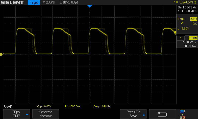
Do you have any possible solution?

Many thanks.

  • Hi Dan,

    For question 1

    The min voltage of VGL is determined by AVDD, diode VF and Rds(on) of IC internal FET.

    For question 2

    Could you please help to capture more figures: 1) AVDD, VGH, VGL and VCOM start-up behavior with normal condition; 2) AVDD, VGH, VGL and VCOM start-up behavior with "fault" condition.

    And have you checked the voltage on VIN and EN during start-up?

    BR

    Patrick

  • Hi,
    thanks for the response.

    For question 1: in another discussion I read this reply:

    "This design s using a single stage of the negative charge pump and with single stage, it is no possible to achieve -13V with AVDD of 8.2V. They need to use two stages for the negative charge pump i.e add one more BAT754S+220nF capacitor at the node LCD_VGL. Connection of the feedback resistor divider network should also be moved to the output after second stage i.e. disconnect R2015 from current connection at Q2003 and connect it to the new connection at the output of second stage."

    But I don't understand how to achieve this.

    For question 2: I found the problem was a voltage spike on Vin.

  • Hi Dan,

    I don't know where you found such discussion, but I suppose the two-stage negative charge pump is probably like this:

    And, after you eliminated the voltage spike, will your system work normally?

    BR

    Patrick

  • Hi,
    sorry but I can't view the image, the web page remains in a loading state.

    For the second question yes, I had voltage spike on a start-up phase that I think they sent to fault state the TPS65100; fixed that everything works fine.

  • Hi Dan

    I re-upload the figure again. Please kindly check if this can be seen.

    BR

    Patrick

