This thread has been locked.

If you have a related question, please click the "Ask a related question" button in the top right corner. The newly created question will be automatically linked to this question.

LM5108: Driver failure

Part Number: LM5108

Hi,

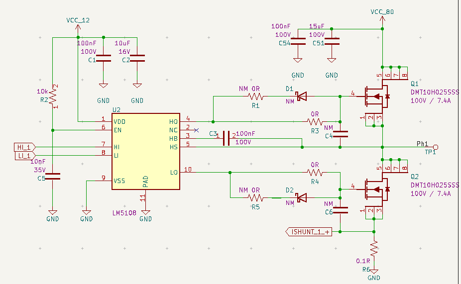
I am currently working on the power control PCB for a FOC controlled BLDC motor. The three phases of the motor are powered using three LM5108 coupled to 6 MOSFETs (1 LM5108 + 2 half bridge MOSFET per phase). PWMs are generated by a micro-controller on the same board.

We are experiencing multiple failures of the LM5108 part on many of our boards (at least 25 of them). I have measured negative transients (-10V) across HO and HS pins during MOS switch-off which are probably linked to the MOS Ciss capacitors + motor coils discharging into the driver while switching. As the HO pin is rated for negative voltages reaching HS-0.3V, I suspect this is the origin of my troubles.

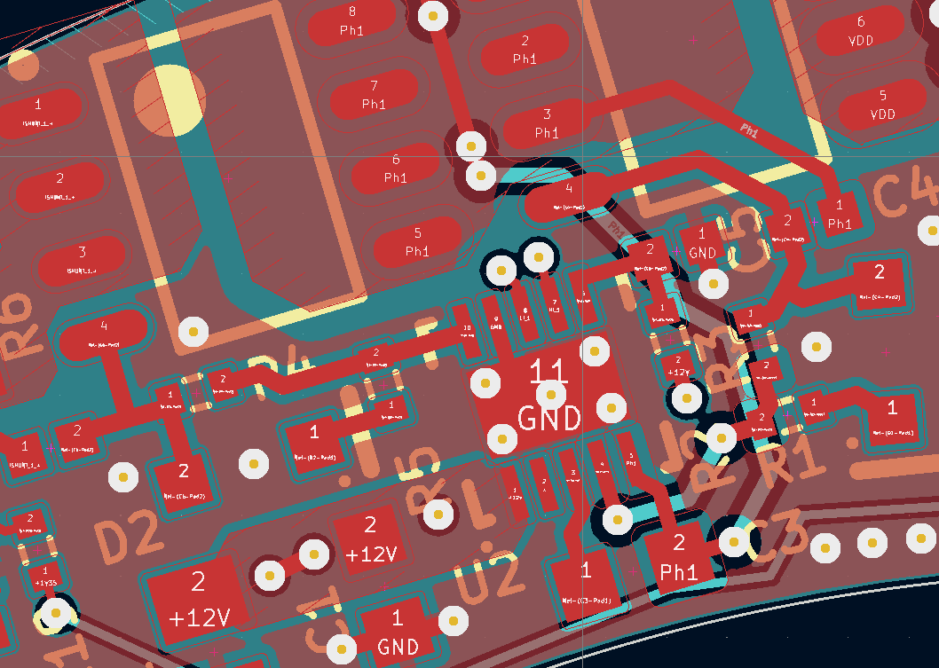
I am planning on adding a series resistance on HO and LO pins to slow the current discharge. I also may add schottcky diodes between HO and VDD and HO and HS (same for LO pin). Could you confirm I am not missing anything here please ? I having included layout and schematic as it may help.

PS: In recent testing, the sub layer (blue) route linking HO (pin 4) to R1 melted and acted like a fuse. Do you think vias/tracks are undersized (vias are 0.15mm drill and 0.5mm diameter, tracks are 0.250mm)? I tried following the datasheet instructions as much as possible.

Thank you in advance for any help you can provide !

Best regards,

  • Hello Maxime,

    Thanks for your interest in this part.

    Adding schottky diodes from HO to HS and HS to VSS would help prevent the negative voltage transients. You don't need a diode between HO and VDD. Increasing the series resistance could help as well.

    I think you could also get improvements from the layout. You can follow the layout in the datasheet as an example. You should try to expand the traces and vias as much as possible. Expanding the traces and vias reduces the inductance which reduces the amount of overshoot you experience. I think it may be possible to also route HO and LO closer to the gates of their transistors. It especially looks like HO can take a more direct path to the transistor if it goes underneath the driver IC.

    Please let me know if you have any more questions.

    Best Regards,
    Ethan Galloway

  • Thanks a lot for your answer. I will try to fit everything in the new design.

    Regarding the schottky diode, is there any specific parameter I must pay attention to ? I am guessing, relatively fast recovery time, low forward drop and able to let pass a fair amount of current (I would say at least one amp minimum).

    Best regards,

    Maxime

  • Hello Maxime,

    Yes, fast recovery time and low forward voltage drop will be necessary. 1 amp of current sounds about right for what you need.

    Best Regards,
    Ethan Galloway

  • Ok I will try all this. Thanks again for your help !

    Best regards,

    Maxime