


Hi,
There is short issue between SW and GND.
Could you help to solve this issue?
condition:
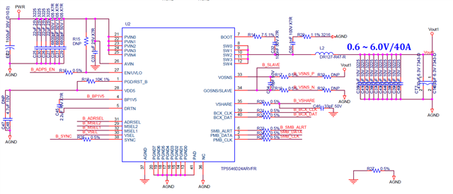
Vin: 12V
Vout: 3.3V
Iout: 40A
Operating: repeat 2s On and 400ms Off
After this operation for few hours, it is operated abnormally. When check impedance between SW and GND, it's short.
Schematic
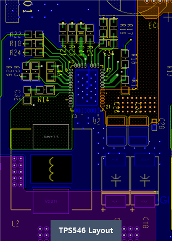
Layout
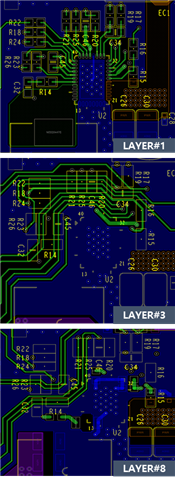
|
LAYER |
Description |
|
LAYER#1 |
Signal |
|
LAYER#2 |
GND (All Plane) |
|
LAYER#3 |
Signal |
|
LAYER#4 |
POWER |
|
LAYER#5 |
GND (All Plane) |
|
LAYER#6 |
POWER |
|
LAYER#7 |
GND (All Plane) |
|
LAYER#8 |
Signal |
Thanks.
