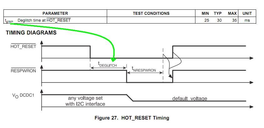
I am using the TPS65023B with a supercap for VBACKUP. I want VLDO1=1.8V and VLDO2=3.3V. I'm using VRTC to power VINLDO and I have the DEFLDO[2..1] pins tied to VRTC. This was working fine on the first cut of the board, but on the second rev it is not. Is this an acceptable way to do this? The new board is powering up with VLDO1= 1.3V and VLDO2=3.3V, which is what should result from DEFLDO[2..1] both being tied low. The only thing I've found in the datasheet is the paragraph on p 25, where it says "the digital value applied to the pins is latched during power up and determins the initial output voltage according to Table 3." Is there some delay in the PFET that switches VRTC to the VSYSIN pin that is somehow causing the inputs to be sampled before VRTC reaches a threshold? If I move the DEFLDO pins to VSYSIN, it works fine. The only other reference I find in the datasheet is in the table on p3. This shows tglitch for DEFLDO1 and DEFLDO2 = 25ms (min) to 35ms (max). The description says "Deglitch time at \HOT_RESET". What exactly does this mean? I don't see it in any of the timing diagrams. To me, this implies that the DEFLDO pins may be latched after the rising edge of \HOT_RESET, which I have pulled up to VRTC. VSYSIN is tied to VCC in my circuit. Does anyone have any information on this?

-
Ask a related question
What is a related question?A related question is a question created from another question. When the related question is created, it will be automatically linked to the original question.