Other Parts Discussed in Thread: PMP9656
Hi TI partner,
Currently, I'm design ACF topology that using UCC2897A for Vin:43V~60V to Vout:12V/21A application, as below is my design questions list, need your help to clarify them.
Q1: refer to PMP9656, the transformer is "RA6992-BL", I want to use "PH0908.002NL" to replace it, need your help to double confirm its spec.
RA6992-BL: Pri-Sec-Aux=8T:4T:4T=> turn ration: 2:1:1; Pri-inductance=50uH https://www.coilcraft.com/en-us/products/transformers/planar-transformers/planar/ra6992/
PH0908.002NL: Pri-Sec-Aux=4T:2T:2T=> turn ration: 2:1:1; Pri-inductance=>211uH/2/2=52.75uH (Pri-A parallel Pri-B) https://productfinder.pulseelectronics.com/part/ph0908nl
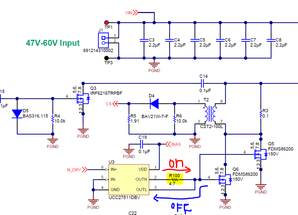
Q2: refer to PMP9656, T2 should be for current sensing, what is the function of R3? Why it parallel with T2 ? As I know, it will separate the current path that flow to T2 & R3 that means T2 will not sense the total current of Q5 &Q6, so the reporting "CS" will be wrong?
Q2-1: If I don't use T2 for current sensing, and I connect a R-sense and series with Q5/Q6 source pin for current sensing. Is it workable? The Cons/Pros is?
Q3: In MOSFET parallel application, we usually series R-Gate in each MOSFET to ensure consistent on/off timing, but in PMP9656 sch, I only see one R-Gate/R100 for Q5/Q6? Why?
Q3-1: R100 place location, seems to make lower turn-on speed and faster turn-off speed, am I right? If not, please correct me.
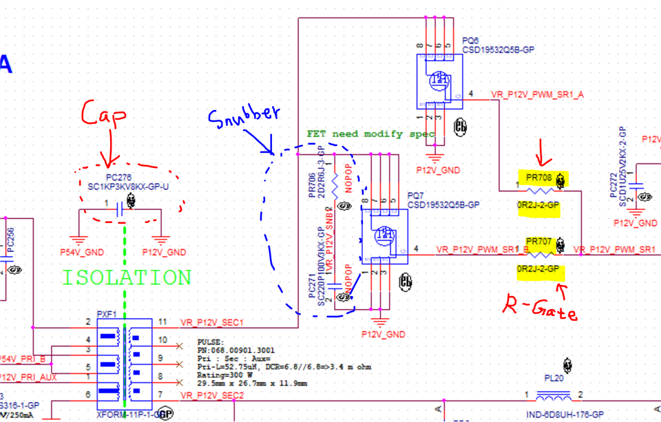
Q3-2: SR FET: Q1/Q2 and Q4/Q7 not seen R-Gate for each FET, is it need to reserve to ensure the consistent on/off timing of parallel MOSFET?
Q4: regarding to EMI testing, since our system need to pass Class-B, is there any solution need to reserve in advance or special layout guideline for this? Please recommend, thanks!
Looking forward your reply!