- Ask a related questionWhat is a related question?A related question is a question created from another question. When the related question is created, it will be automatically linked to the original question.
When using the LM5100AM Gate Driver according to the typical application circuit shown in the data sheet, LO and HO signals when probed do not show the expected outputs. I believe this must be due to a mistake on my end but cannot figure out why. When probed, LO is always equal to GND, and HO is always equal to VIN (the driving voltage).
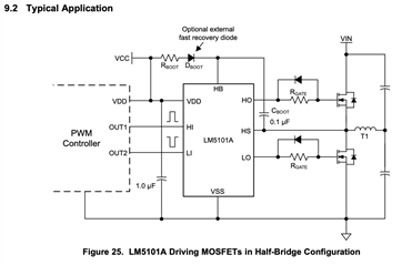
Here is the typical application schematic as shown in the IC's data sheet.
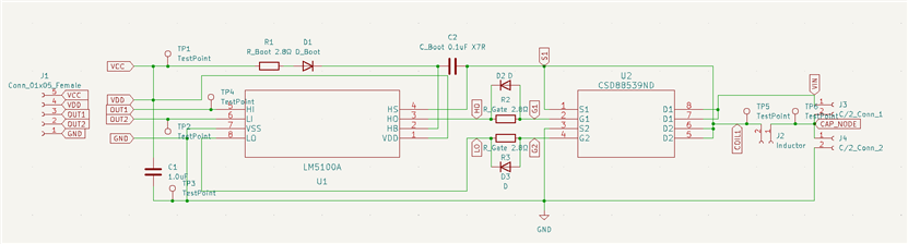
And here is an image of my circuit schematic (u2 is a TI dual mosfet IC, the CSD88539ND):
In testing I supplied VCC (and by extension VDD) and VIN with 12V. HI was supplied with a 3.3V 150kHz square wave generated by an STM32G0 microcontroller, and LI was supplied with the same signal that had been inverted. Probing HI and LI showed that LI was indeed correctly inverted and timing was well within good range.
Although all these values seem to be well within the ranges stated in the data sheet, HO always outputted the same 12V signal as VIN, and LO always outputted GND.
With this information, is there any reason why the driver HO and LO outputs would not have the expected signals? Happy to provide any additional information at your request.
Looking forward to any responses, and thanks in advance!