This thread has been locked.

If you have a related question, please click the "Ask a related question" button in the top right corner. The newly created question will be automatically linked to this question.

TPS63900: TPS63900DSKR Unexpected failure

Part Number: TPS63900

Hi to everyone we are testing the TPS63900DSKR in the following conditions and with the following part failures. Any advice on why this could happen?

Failure type 1 (2 devices broken in this condition):

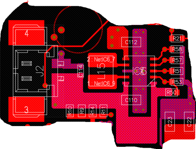
  • Device input voltage 4.5V
  • Output V2 set to 3.3V with no current limitation
  • Output V1 set to 3.3V
  • Total Capacity on Vout about 850uF (ceramic capacitors)
  • 2.2uH coil
  • SEL INPUT connected to Vin
  • EN PIN set to VIN
  • CFG1 with 36.5 KOhm 1% resistor to GND
  • CFG2 with 0 Ohm to GND
  • CFG3 with 16.2 KOhm 1% to GND
  • Output current load about 4mA (before failure)
  • Input power supply: Laboratory DC power supply max 3.5A output

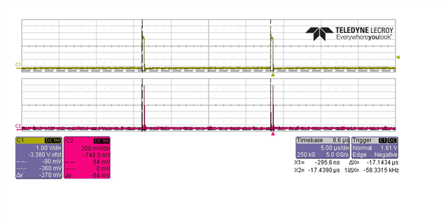
In this condition the part fails after few minutes of operation with no action. Output is shorted to GND. >2A absorbed from input power supply 

Failure type 2 (2 devices broken in this condition):

  • Device Vin input voltage 3.8V
  • Output V2 set to 3.3V with no current limitation
  • Output V1 set to 3.3V
  • Total Capacity on Vout about 850uF (ceramic capacitors)
  • 2.2uH coil
  • SEL INPUT connected to Vin
  • EN PIN set to VIN
  • CFG1 with 36.5 KOhm 1% resistor to GND
  • CFG2 with 0 Ohm to GND
  • CFG3 with 16.2 KOhm 1% to GND
  • Output current load about 4mA (before failure)
  • Input power supply: Laboratory DC power supply max 3.5A output 

In this condition the part fails after few minutes of operation with no action. Output goes to 0.5V. about 50mA absorbed from input power supply.

Thanks Jan

  • Hi  Jan,

    Thanks for your detailed description.

    according your description, i suspect there is a big parastic inductor in your layout and some circuit inertal damaged.

    could you share your layout here?

    Regards

    Tao

  • Hello Tao,

    thanks for your reply.

    Below I send you the layout of the regulator region on our board. The signal Vbat is connected to J2 through a short cable (<6cm)

    GND is on internal Layer 2  connected with vias as shown underneath IC6 (TPS63900DSKR)

  • Hi Tao,

    is there a way to have a direct contact with TI technical assistance?

    Thank Jan

  • Hi  Jan,

    Webex meeting is suitable for you? if so, i will send you a link and then we can have a meeting directly.

    Regards

    Tao

  • Hi Tao,

    that would be great. Many thanks. So we can share screens. If possible for you we could we arrange for toady in early afternoon CET?

    Jan

  • Hi  Jan,

    how about 1.00PM CET?  if it is available, you can join by the link below.

    https://ti.webex.com/meet/tao-zhang

    Regards

    Tao

  • you are welcome. see you.

  • Hi Jan,

    thanks for considering our devices.

    could you help to do another check after you remove the damaged device from board. may be you can find some abnormal impendance between PINS. espicially the impendance between pin Vin/Vout/L1/L2 to GND.

    Regards

    Tao

  • Hi,

    below impedance measurement (device not powered) on the broken device:

    L1 to GND :0.9Ohm

    L2 to GND :0.8Ohm

    Vin to GND : open circuit >3MOhm

    Vout to GND : 0.7MOhm rising (I see output capacitors charging, the multimeter is charging the capacitors )

    Oscilloscope measurement on the same part

    C1 Voltage measured on L1 (Vin=4.5V)

    C2 Output voltage Vout=0.035V

    Switching frequency measured 58KHz

  • Hi,

    impedance measurement on not broken device:

    L1 to GND : about 70KOhm

    L2 to GND :70K Ohm

    Both slowly decreasing

  • Hi  Jan,

    Seems you did not remove the device from the board when you  do the impendance measurement and the oscilloscope measurement is based on the damaged device, right?

    Regards

    Tao

  • Hi,

    yes correct the oscilloscope measurement is on the broken device and the impedance measurement is done without removing the device.

    I will repeat the impedance measurement removing the inductor I have the suspect that one of the mosfets is broken.

    regards and thanks

    Jan

  • Hello Tao,

    I show you my impedance measurements on L1 and L2 on the broken TPS63900 Inductor removed from circuit:

    L1 (PIN9) to Vin => Open (2Mega Ohm)

    L1 (PIN9) to GND => Open (2Mega Ohm)

    L2 (PIN7) to VIN => Open (2Mega Ohm)

    L2 (PIN7) to GND => Short (1Ohm)

    L2 (PIN7) to VOUT => Open

    According to the "Power Stage Simplified Block Diagram" shown on the part data-sheet it seems to me that Q3 is broken. 

    I will make the same measurements on the other broken parts.

    Any hint on how this could happen?

    Best regards

    Jan

  • Hi  Jan,

    thanks for your great work.

    yes, you are correct, the Q3 may demaged and mostly it is caused by the high spikes during the switching.

    with 4.5V input, device should always work in buck mode and there will be no switching in node L2, because Q3 is always off and Q4 is always on.

    so here i suspect two root cause as bleow.

    • input is bulit up with a small slew rate, then, during start-up, device may run into Buck-Boost mmode.
    • there may be some oscillation at the output, since there are many caps far away from device, i think it is resonable and we can confirm by adding some more caps near the device.

    Regards

    Tao

  • Hi Tao,

    many thanks for your help I will follow your advises.

    I have analysed the other two broken parts in the same way. They are broken in a different manner:

    Part2: Vin 4.5V, Vout 0.04V, I input = 176mA

    L1 (PIN9) to Vin => Open
    L1 (PIN9) to GND => 5Ohm
    L2 (PIN7) to VIN => Open
    L2 (PIN7) to GND => Short (1Ohm)
    L2 (PIN7) to VOUT => Open

    Part 3: Vin 4.5V, Vout 0.5V, I input = 3A (Power supply limit)

    The input power supply voltage drops to 2.5V because in is limited to 3A (I assume that this changes the switching behaviour and it tries to go to boost mode)

    L1 (PIN9) to Vin => Short
    L1 (PIN9) to GND => 10Ohm
    L2 (PIN7) to VIN => 11 Ohm
    L2 (PIN7) to GND => Short (1Ohm)
    L2 (PIN7) to VOUT => Open

    Do these measurement confirm you failure root causes?

    Thanks regards

    Jan

  • Hi  Jan,

    i am not very sure, but i think we can do follows to confirm.

    • Enable the device when input is built up already. if you can confirm that device start to switching after vin is 4.5V already. we can ignore it.
    • add more output caps close to device.

    mostly, i think the issue should be fixed.

    some other measurement with oscilloscope we do is with the good device and board. catch the node L1 Vout VIn, and trigger with the falling eage of Vout.

    then, i think we can get more info about the root cause of this failure

    Regards

    Tao

  • Hi,

    surly our device will start switching before input voltage is stable.

    It will not be possible for us to enable the device only when input voltage is stable. In order to do this we would need to use some sort of voltage monitor to enable switching, but in a battery operated product this is very difficult because you don' know the voltage of the battery that is being used. User could plug in a semi-empty battery and in this scenario it wont be possible to  set a voltage threshold for the voltage monitor that ensures a stable input voltage in all conditions.

    Is it mandatory to enable the device only when input voltage is stable for correct operation of the voltage regulator?

    Jan

  • Hi   Jan,

    yes, just want to confirm if the device damaged in buck mode or not.

    Regards

    Tao

  • Hi Tao,

    I forced EN PIN 1 to GND to disable the device on part 3, Just for reminder part 3 failure mode:

    Part 3: Vin 4.5V, Vout 0.5V, I input = 3A (Power supply limit)
    The input power supply voltage drops to 2.5V because in is limited to 3A (I assume that this changes the switching behaviour and it tries to go to boost mode)
    L1 (PIN9) to Vin => Short

    L1 (PIN9) to GND => 10Ohm
    L2 (PIN7) to VIN => 11 Ohm
    L2 (PIN7) to GND => Short (1Ohm)
    L2 (PIN7) to VOUT => Open

    The result is the same, I see high current (3A) drawn from my power supply even the regulator is disabled. It seems that mosfets on input side Q1 and Q2 are damaged.

    In my next post I will try do the same test on device 1.

    Jan

  • Hi Jan.

    do you use a long cable in your tests? i mean a long cable from your power supply and your board.

    is it possible you can send me a board?

    Regards

    Tao

  • Hi,

    the cable from the power supply to the board is about 1meter long. I have done some measurements to investigate some input voltage overshot do to cable or power supply inductance. I did not see any dangerous voltages.

    I will check if I can send you the board. Would you like to investigate one board with the broken parts, too? How should I prepare the board, do you prefer that I will isolate EN pin from Vin?

    Thanks

    Jan

  • Hi  Jan,

    with your orginal design is ok. no need to isolate the Pins.

    my address is below.

    2/F NO. 72 Liangxiu Road

    Pudong New Area, Shanghai, 201203 

    Tao-Zhang  +86-15258838463

    Regards

    Tao

  • Hi Tao,

    thank you, would it be possible for you to send us a non disclosure agreement?

    Jan

  • Hi  Jan,

    I did not do this before and i suspect there will be a big delay caused by business reasons.

    we can still observe the unexpected failure with good device, right?

    if so, i think the best way to solve this problem is that we can catch the waveform at the damaged moment. with the info of VIn  Vout and LX1. 

    Regards

    Tao

  • Hi,

    I understand, I will double check if non disclosure is necessary for our company in this case. In the meantime I will try to catch the failure as suggested by you.

    Please do not close this thread until you receive any further news from me.

    Thanks again for your help.

    Jan

  • Hi  Jan,

    of course. i will keep it open or transfer the status to waiting for customer.

    Regards

    Tao