This thread has been locked.

If you have a related question, please click the "Ask a related question" button in the top right corner. The newly created question will be automatically linked to this question.

LM5025: AGND / PGND / Power-GND connection

Part Number: LM5025

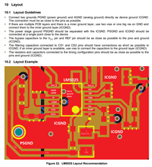
the datasheet of LM5025 says to connect AGND and PGND as close as possible to the LM5025 pins.

PGND seems to be used only for the gate driver.

So if i use a current sense resistor between the (OutA) FET-S and Power-GND, why is PGND not connected directly to the FET? 

CS1 and CS2 are only 0.25V relative to AGND. So should the connection between AGND and Power-GND be near the current sense resistor?

Also what is the maximum allowed voltage difference between AGND and PGND? 

  • Hello M W

    The LM5025 datasheet has a PCB layout guideline that addresses grounding.  See below.  The AGND and PGND pins are adjacent and should have extremely low differential voltage between them.

    Regards,

    Eric

  • Hi Eric,

    this sniplet of the datasheet was the reason for my posting in this forum.

    The reference design kind of avoids my problem by using a current transformer instead of a sense resistor. That current transformer is placed on the high side of the switching FET. 

    My problem using a sense resistor is, i need something like 20..50mohm. But the actual sense voltage includes the trace between the sense resistor and AGND-pin. That adds another 10..20mohm, with a complex (inductive) part. And the gate drive pulse is pushed through the sense resistor+trace. As a result, the gate drive triggers CS1/CS2.

    My thinking was to remove the gate drive pulse from the sense resistor, but that would mean 20..50 mohm and some trace length between AGND and PGND.

    Now if the AGND/PGND connection at the LM5025 pins is a strict requirement, i see no solution but to do a bigger redesign.

    Best Regards

    Matthias


  • Hi M W,

    Thanks for clarifying.  I understand now.

    Are you sure it's the gate drive pulse triggering CS1/CS2?  It's probably the MOSFET turn-on.  The di/dt spike from the MOSFET is well known issue.

    To deal with MOSFET turn-on spike we usually:

    1) Use a filter at the CS pins.  If you already have an RC filter can you increase the values to produce more filtering?

    2) Slow down MOSFET switching speed with a gate resistor.  Do you have or can you introduce a gate resistor and slowly increase the value (2, 4, 6...etc)?

    Regards,

    Eric

  • Hi Eric,

    i already have an RC filter at the CS pins. Switching frequency is ca. 300khz. On CS1 i have 10k/10pF. On CS2 i have 10k/10nF. Both CS1 and CS2 get triggered.

    I do not currently have a gate resistor. I do have the Power-GND on a separate PCB trace from PGND. 

    My layout currently is probably not 100% optimal, the sense resistors are near CS1/CS2, there is some PCB path to the other side of the LM5025-AGND/PGND. That AGND/PGND path is currently common between gate-drive and CS1/CS2 sense, as required by the AGND/PGND connection. I suspect the gate drive pulse lifts that common GND. So my idea was to have the gate drive PGND removed from the sense resistors and AGND.

    I cant be sure, if the gate drive pulse or the turn-on spike causes this. However the main power path through the MOSFET is limited by the inductivity of the transformer, the gate drive pulse is not. So currently i suspect the gate drive.

    Best Regards

    Matthias

  • Hi Matthias,

    We usually use 1k and 100pF-220pF to filter the CS information.  CS1: 10k and 10pF has the same time constant/break frequency as 1k and 100pF.  CS2: 10k and 10nF is quite a bit of filtering and I wonder how it would ever trigger via CS2.

    If there is any stray capacitance from the MOSFET drain to ground the current sense will see a spike when the MOSFET turns on and discharges the parasitic capacitance.  I've used a differential probe to measure directly across the CS pin capacitor to see if I have enough filtering.  Do you have a differential probe, such as Tektronix P6247?

    It's a little difficult to understand your exact grounding scheme.  In general, removing PGND from AGND makes sense.  You should create an island (polygon pour) for AGND.  Also, create a separate island (polygon pour) for PGND and connect the input capacitors, PGND pin, and sense resistor grounds.  Finally, connect AGND and PGND together at a single point.

    This datasheet (Section 9.3, page 41) has a very good detailed example of a PCB layout (with pictures) for a flyback.  Make note of the use of a single-point ground connection for AGND and PGND.  Also, minimize the loop(s) as shown in the example.

    Good luck,

    Eric

  • Hi Eric,

    thanks for taking your time to help me.

    My design has some distance between the current sense resistor and the star GND point. That seems to be the problem. My current sense resistor is near CS1/2 pin, the star GND is at AGND/PGND pin (on the other side of the LM5025). The design from the linked datasheet has the current sense resistor very close to the star GND.

    I dont have a proper diff probe. But for a test at the CS2 RC filter i replaced the C with a 0R resistor (CS2 to GND). This also triggers CS2. CS2 is not triggered, if i bodge a wire above the LM5025 case between CS2 and AGND. So my GND is bad at the point where the current sense resistor is...

    Thanks for your help.

    Matthias