Dear Sir:
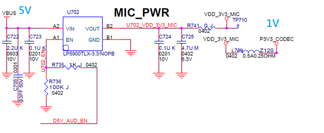
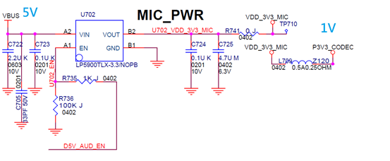
LP5900TLX-3.3
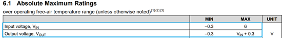
VIN: 5V
EN: Low
VOUT: 1V
VOUT Absolute Maximum Rating : VIN(max)+0.3 =6+0.3=6.3V
When the voltage of VOUT is 1V. < VOUT(Max) = 6.3V
It doesn’t cause the damage LP5900TLX-3.3(U702)
Is it correct?
Please check to reply it asap.
Thanks
B,R
Vincent