This thread has been locked.
If you have a related question, please click the "Ask a related question" button in the top right corner. The newly created question will be automatically linked to this question.
Hi.
Could this be revised by an engineer of Texas Instruments?
I'm open for tips and suggestions.
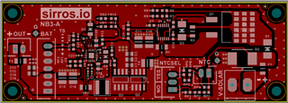
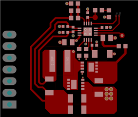
The initial schematic is attached.
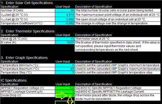
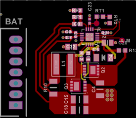
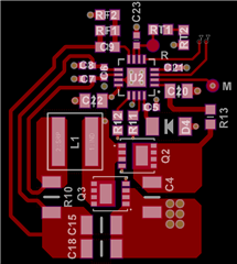
MPPSET PIN RESISTORS
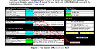
It will be initially considered a 36-cell solar panel with a MPP (maximum power point) voltage of 18.54V. 3 resistors will be used to make a divider between the solar panel voltage and the MPPSET pin of BQ24650, 3 resistors to give more flexibility for future combinations. A resistor divider that when the solar panel has 18.54V (MPP voltage), the MPPSET pin has 1.2V.
Resistors relation = (18.54-1.2) / 1.2 = 14.45
Resistors = 4.7K and 68K (68K + 0R)
The tolerance of the resistors will be 0.1% (4.7K and 68K)
Vmpp(min) = 1.2+1.2*( (68*0.999) / (4.7*1.001) ) = 18.527V
Vmpp(typ) = 1.2+1.2*(68/4.7) = 18.562V
Vmpp(max) = 1.2+1.2*( (68*1.001) / (4.7*0.999) ) = 18.596V
VFB PIN RESISTORS
VBAT = 2.1 + 2.1 * (Rup / Rdown)
It will be used a Li-ion battery with 4.2V floating voltage, so the resistors just need to have the same value. At first, it will be used 2 resistors of 47K with 0.1% tolerance.
Leakage current into VFB pin = 100nA max
SHUNT RESISTOR
SRP-SRN current sense voltage = 40mV +- 3%
40mV / 2.5A = 40 / 2.5 = 16mR
Shunt commercial value = 15mR 1%
40mV / 15mR = 2.66A
I_charge(min) = (40*0.97) / (15*1.01) = 2.56A
I_charge(typ) = 40/15 = 2.66A
I_charge(max) = (40*1.03) / (15*0.99) = 2.77A
(2.77^2) * (15*0.99) = 114 mW, can be used a 1206 resistor of 1/2W
INDUCTOR SELECTION
Initially it will be considered the inductor below, which is already used by us in another board:
Inductor microHenry, SMD, 10uH, +-20%, 5.2A current rating, 9.1A saturation current, shielded, 45.76mOhm max, -55°C ~ 155°C, 8.5x8x5mm, ETQ-P4M100KVK (Panasonic).
The maximum inductor ripple current happens with D = 0.5 or close to 0.5. Usually inductor ripple is designed in the range of 20% to 40% of the maximum charging current as a trade-off between inductor size and efficiency for a practical design.
I_ripple = V_in * D * (1-D) / ( fs * L )
I_ripple = 27.57 * 0.5 * (0.5) / ( 600000 * 10*10^-6 )
I_ripple = 1.15A
I_sat >= Ichg + 0.5*(I_ripple)
I_sat >= 2.77 + 0.5*(1.15)
I_sat >= 3.35A
Ok, the inductor chosen has an I_sat of 9.1A. Maybe it can be replaced by a smaller inductor with smaller saturation current, to reduce the size of the solution.
RESISTORS AT TS PIN
It was considered the use of the thermistor 103AT-2, and a safety charge temperature from 0°C to 45°C
RTHcold(°0C) = 27.28K
RTHhot(°45C) = 4.911K
VREF = 3.3V
VLTF = 73.5% of VREF (3.3V) [typ] = 3.3*0.735 = 2.426V
VTCO = 45% of VREF (3.3V) [typ] = 3.3*0.45 = 1.485V
RT2 = ( VREF * RTHcold * RTHhot * ( (1/VLTF) - (1/VTCO) ) ) / ( (RTHhot * ( (VREF/VTCO) - 1)) - ( RTHcold *( (VREF-VLTF) -1 ) ) )
RT2 = ( 3.3 * 27280 * 4911* ( (2.426) - (1/1.485) ) ) / ( (4911 * ( (3.3/1.485) - 1)) - ( 27280 *( (3.3-2.426) -1 ) ) ) = 82083 Ohms
RT2 commercial = 82K
RT1 = ( (VREF/VLTF) - 1 ) / ( (1/RT2) + (1/RTHcold) )
RT1 = ( (3.3/2.426) - 1 ) / ( (1/82000) + (1/27280) ) = 7.374K
RT1 commercial = 7.5K
MPPT TEMPERATURE COMPENSATION
The compensation for the ambient temperature of the solar panel is still not included, could the LM234 be supplied through the rail "LT-VOUT" of my schematic?
I have some doubts.
(1) How to calculate or, for my case, what should be the value of the feedforward capacitor, C17
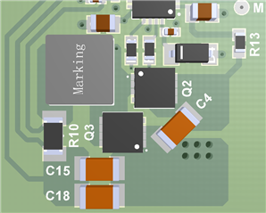
(2) For transistors Q2 and Q3, AO4484, should I replace them with others with a bigger package like the TO-252 (DPAK)? Or are they suitable? Because by reading the datasheet of BQ24650 I ended up understanding that it drives the Mosfets with small Vgs voltages, not like ~12V Vgs drive.
Regards,
Jeferson.
Hello Jeferson,
Please see my comments in order:
MPPSET Resistors - I agree with the calculations of the MPPSET point for the resistors.
VFB Pin Resistors - I agree with the scheme, but I would recommend increasing the value of resistance. This will be a constant discharge path via voltage divider from battery voltage in addition to the leakage you cited. In Figure 15 Typical Application the total divider resistance is 600 kOhm (a factor of 6.3x more resistance helping to decrease battery discharge).
Shunt Resistor - I agree with the calculations.
Inductor Selection - The inductor could definitely be reduced, saving some DCR and size along the way.
Resistors at TS Pin - My only comment would be to take into account VHTF, which has a slightly narrower region to start charge. Please check that the commercial resistors yield the desired TS settings.
MPPT Temperature Compensation - Yes that is where the LM234 would connect. Please see Figure 18 for VCC Resistor and Capacitor.
Doubt 1 - We use 22 pF in Typical Application, but due to RC behavior the size of the capacitor will affect how fast or slow the VFB is realized in response to changing battery voltage.
Doubt 2 - The package size is a tradeoff between heat dissipation, size, and cost. Please evaluate accordingly.
Other Notes:
1. C6 not needed on SRP. C16 0.1 uF is for common mode filtering.
2. We recommend minimum 15 uF output capacitance on SRN for 2 A charge current and higher.
Regards,
Mike Emanuel
Hi Michael.
Thank you so much.
About your comments:
MPPSET Resistors - I agree with the calculations of the MPPSET point for the resistors.
Ok.
VFB Pin Resistors - I agree with the scheme, but I would recommend increasing the value of resistance. This will be a constant discharge path via voltage divider from battery voltage in addition to the leakage you cited. In Figure 15 Typical Application the total divider resistance is 600 kOhm (a factor of 6.3x more resistance helping to decrease battery discharge).
I have placed two 300K resistors for the divisor this time.
Shunt Resistor - I agree with the calculations.
Ok.
Inductor Selection - The inductor could definitely be reduced, saving some DCR and size along the way.
Ok.
If use 4.7uH inductor
I_ripple = V_in * D * (1-D) / ( fs * L )
I_ripple = 27.57 * 0.5 * (0.5) / ( 600000 * 4.7*10^-6 )
I_ripple = 2.44A
I_sat >= Ichg + 0.5*(I_ripple)
I_sat >= 2.77 + 0.5*(2.44)
I_sat >= 4A
Possibility: Inductor microHenry, SMD, 4.7uH, +-20%, 5.9A current rating, 8.2A saturation current, shielded, 36.3mOhm max, -55°C ~ 155°C, 5.5 x 5.3 x 3.1mm, SRP5030CA-4R7M (Bourns).
Resistors at TS Pin - My only comment would be to take into account VHTF, which has a slightly narrower region to start charge. Please check that the commercial resistors yield the desired TS settings.
Ok, you say about Figure 10. I understand. Noted.
RESISTORS AT TS PIN (RECALCULATION)
My equations for calculating RT1 and RT2 were wrong, now they are correct. And you can see at the end that considering the values of RTHcold and RTHhot of thermistor 103AT-2, and considering the calculated values of RT1 and RT2, the low temperature (ºC) and high temperature (45ºC) thresholds match voltages VLTF and VTCO.
RTHcold(°0C) = 27.28K
RTHhot(°45C) = 4.911K
VREF = 3.3V
VLTF = 73.5% of VREF (3.3V) [typ] = 3.3*0.735 = 2.4255V
VTCO = 45% of VREF (3.3V) [typ] = 3.3*0.45 = 1.485V
RT2 = ( VREF * RTHcold * RTHhot * ( (1/VLTF) - (1/VTCO) ) ) / ( (RTHhot * ( (VREF/VTCO) - 1)) - ( RTHcold *( (VREF/VLTF) -1 ) ) )
RT2 = ( 3.3 * 27280 * 4911* ( (1/2.4255) - (1/1.485) ) ) / ( (4911 * ( (3.3/1.485) - 1)) - ( 27280 *( (3.3/2.4255) -1 ) ) ) = 30115.15 K Ohms
RT2 commercial = 30K
RT1 = ( (VREF/VLTF) - 1 ) / ( (1/RT2) + (1/RTHcold) )
RT1 = ( (3.3/2.426) - 1 ) / ( (1/30000) + (1/27280) ) = 5.147 K Ohms
RT1 commercial = 5.11K
Calculating back:
RTHcold(°0C) = 27.28K
RTHhot(°45C) = 4.911K
RT1 = 5.11K
RT2 = 30K
(1) low temperature threshold.
30K // 27.28K = (30*27.28) / (30+27.28) = 14.287K
3.3V * ( 14.287K / (14.287K + 5.11K) ) =
3.3 * ( 14.287 / (14.287 + 5.11) ) = 2.43V (very close to VLTF...)
(2) high temperature threshold.
30K // 4.911K = (30*4.911) / (30+4.911) = 4.22K
3.3V * ( 4.22K / (4.22K + 5.11K) ) =
3.3 * ( 4.22 / (4.22 + 5.11) ) = 1.49V (very close to VTCO...)
VHTF = 47.5% of Vref [typ] = 0.475 * 3.3 = 1.5675V
3.3 * ( x / (x + 5.11) ) = 1.5675
x = 4.6235K (parallel of thermistor and RT2)
30K // y = (30*y) / (30+y) = 4.6235K [x]
y = 5.466K
VHTF (calculating back)
30K // 5.466K = (30*5.466) / (30+5.466) = 4.6235K
3.3V * ( 4.6235K / (4.6235K + 5.11K) )
3.3 * ( 4.6235 / (4.6235 + 5.11) ) = 1.5675 (match voltage of VHTF)
So, when the resistance of the thermistor is 5.466K, the voltage at TS pin will be equal to 1.5675V, which is the typical voltage VHTF. Datasheet of the thermistor:
5.466K is between 40 to 45ºC. It is something about 40.5°C to 42.5°C (max) to be able to initiate a charge, and 39~40°C would be enough.
MPPT Temperature Compensation - Yes that is where the LM234 would connect. Please see Figure 18 for VCC Resistor and Capacitor.
Schematic updated regarding this. What is your opinion?
Rset = 215R
R3 = Rset * ( (2mV * number of solar cells in series) / 227uV )
R3 = 215 * ( (2*36) / 227*10^3 ) = 68.193K = 68K
Rset was chosen as 215R in order R3 results 68K, to match the R15 value of the current schematic.
Iset(25°C) = 0.0677V / Rset
Iset(25°C) = 0.0677 / 215
Iset(25°C) = 314 uA
R4 = (VMPPset * R3) / ( ( VMP_25°C + (R3 * (0.0677 / Rset) ) ) - VMPPset )
R4 = (1.2 * 68000) / ( ( 18.54 + (68000 * (0.0677 / 215) ) ) - 1.2 )
R4 = 2105 Ohms = 2.1K
There is a 3 pin pin header (identified as SEL). Connection is among pins 1 and 2 if LM234 is not used, connection is among pins 2 and 3 if LM234 is used. This is because there will be cases that will not have the monitoring of the ambient temperature of the solar panel, and in other cases will have.
Doubt 1 - We use 22 pF in Typical Application, but due to RC behavior the size of the capacitor will affect how fast or slow the VFB is realized in response to changing battery voltage.
Then, for C17, I will begin with 22pF in the first prototype. It will have 0603 package, just because it is easier to swap by another 0603 capacitor by soldering by hands. But if you say than using a 0402 size would be much better in this case, then I will use a 0402.
Doubt 2 - The package size is a tradeoff between heat dissipation, size, and cost. Please evaluate accordingly.
Ok.
Other Notes:
1. C6 not needed on SRP. C16 0.1 uF is for common mode filtering.
C6 (10uF) was removed from SRP.
2. We recommend minimum 15 uF output capacitance on SRN for 2 A charge current and higher.
Ok, added more capacitance to SRN.
Regards.
About the temperature compensation for the solar panel using the LM234, the calculated R4 of datasheet is 2105 Ohms if R3 = 68K. The 3-pin pin header of the previous schematic could be replaced with a 2-pin pin header in order that when it has a jumper connected to it, the parallel of R16 and R21 of my previous schematic yields around 2105 Ohms. In the schematic of my previous post, if somebody forgets to place a jumper on the 3-pin pin header, then the voltage at the MPPSET pin could reach the voltage of the solar panel directly, with the 68K in series and with no resistor pulling the MPPSET pin voltage to ground. The MPPSET pin absolute maximum voltage is 7V.
4700R // x = 2105R
(4700*x) / (4700+x) = 2100
x = 3813R = 3.83K
Calculating back
R3 = 68000 Ohms
R4 = 3.83K // 4.7K = (3.83*4.7) / (3.83+4.7) = 2110.3 Ohms
R4 = (VMPPset * R3) / ( ( VMP_25°C + (R3 * (0.0677 / Rset) ) ) - VMPPset )
2110.3 = (1.2 * 68000) / ( ( VMP_25°C + (68000 * (0.0677 / 215) ) ) - 1.2 )
VMP_25°C = 18.455V (ok)
This way:
Regards.
Hi Jeferson,
Mike is out until Monday. I have reviewed this and in general, I understand what you are trying to do. There is a spreadsheet that you can use to recheck your earlier calculations at
https://www.ti.com/lit/zip/sluc175
I do not understand the use of the LM234 for temperature compensation and am concerned that the MPPSET pin will be overvoltaged if the LM234 is connected to VCC.
Below is an appnote and related spreadsheet that explains how to add a thermistor in series with the MPPSET resistor for temperature compensation.
https://www.ti.com/lit/an/slua586a/slua586a.pdf
https://www.ti.com/lit/zip/sluc175
Regards,
Jeff
Hi Jeff, thanks!
My previous calculations does match with the calculations of the BQ24650 spreadsheet, so that's fine.
But I'm not finding the following spreadsheet, that is the calculator for using NTC for temperature compensation for the solar panel:
In the document that explain it, I did not see a link for the spreadsheet file itself.
Could you please supply me such spreadsheet?
Regards.
Hi Jeff.
Here is the updated schematic and pictures of the initial layout.
Also is attached the spreadsheet with calculations of the resistors for the ambient temperature compensation with the NTC 103AT-2.
Question: In case of reverse polarity at the input of the PCB (up to 60V reverse), for D7, on MPPSET pin, would it be good to use a very low VF, ultra-low leakage shottky diode? -0.3V is the maximum absolute negative voltage at MPPSET pin according to the datasheet of BQ24650. Or maybe, to multiply the values of resistors RP2 (68K) and RP3 (4.7K) by 10 times? To 680K and 47K?
Geo_MPPT_NTC_103AT-2_solar_panel_Resun_RSM060-P_-mppTrackingWithBQ24650AndNTCthermistor.xls
L1: Top Layer
L2: Ground Plane, 0.18mm below L1 (Top Layer)
L3: Signals and GND filling
L4: Bottom Layer, 0.18mm below L3
Top Layer ground
Do you have some observations to make?
Regards.
For good EMC performance, the negative of input filter capacitors, negative of low-side transistor, and negative of output filter capacitors should form a local ground with a star connection, and then connect to the ground plane, no?
Regards.
Hi,
Can you please confirm what second temperature you are using to calculate the temperature coefficient so I can verify the calculation?
In the event of reverse polarity you need to protect all pins connected to the input (in your case MPPSET, VCC, STAT1, and STAT2). Please see Figure 16 which shows a diode D1 to protect for "reverse voltage protection for the VCC pin."
My layout review is as follows:
1. It does not look like there is a separate analog GND and power GND. Please see the separation in Figure 15 in the datasheet and Layout Guideline 7.
2. We recommend in Layout Recommendation 2 for the "gate drive signal traces kept short for a clean MOSFET drive." I believe it would help to shorten the gate drive traces. See our layout in the BQ24650EVM.
Regards,
Mike Emanuel
Hello Michael.
Thanks very much.
Basically I understand ,(1) there is not a separation between analog GND and power GND and (2) gate traces are not short.
Soon I will be able to work in this layout again, then I will check carrefuly.
Regards.
Hi.
This board that I have posted pictures of, is to be supplied by a solar panel with around 18.54V of MPP voltage, and it has a circuit based on IC BQ24650 to charge a 3.7V / 4.2V Li-ion battery, this battery will be supplying another PCB at the same time (a second board, an application board).
Suppose a charge cycle ends, the BQ24650 will switch off, the battery will continue supplying the second board, and after the voltage of the battery drops a few percent from the float voltage (4.2V) the BQ24650 will trigger a new recharge cycle, correct? This way, there will probably exist frequent discharge-recharge cycles which could reduce the lifetime of the battery (I suppose this is true).
The "second board", the board that is supplied by the battery, its supply range would be from 2.7V to 5.5V (its input supply has a TPS63802). I wonder how I could use the power directly from the solar panel to supply the second board, and when this voltage is not present or low enough, then the battery supplies the voltage, and maybe at the same time keep the MPP voltage on the solar panel while the battery is being recharged by the BQ24650 (through its control of the charge current).
I'm in doubt. For example, I wonder if it is possible that the solar panel powers the "second board / application board" and still the BQ24650 be able to recharge the battery controlling the charge current in order to maintain the MPP voltage on the solar panel, or something in this sense / direction.
Any suggestions, tips?
Regards.
Hello,
Someone will get back to you by Wednesday. We are observing President's Day.
Regards,
Mike Emanuel
Hello,
As shown in Section 8.3.5 Charge Termination and Recharge:
A new charge cycle is initiated when one of the following conditions occurs:
• The battery voltage falls below the recharge threshold
• A power-on-reset (POR) event occurs
• MPPSET falls below 75 mV to reset charge enable
If you want to disable charge until a lower voltage you can pull down the MPPSET pin below 75 mV.
The simplest way to handle this is via diode-or. However you will also need a step down converter for the "second board" as you cannot directly connect 18 V to the 2.7V to 5.5V input. First, you would have the step down converter. Then at the output of that converter you would have a diode connection from that to the "second board." In addition, you would have a diode from the battery to the "second board." Whichever voltage is higher will supply the "second board."
Another key thing you need to keep in mind here is that the BQ24650 does not regulate a separate system rail from the battery. The function of the charger is to charge the battery. If the battery is being charged while the "second board" is loading the battery this will interfere with the expected charge time, how much current goes through the inductor, etc. and the use case/characteristic of such a draw needs to be investigated according to your application.
Regards,
Mike Emanuel
Hi Michael, thanks for helping.
Yes, there is the idea of the extra buck converter with O'ring with diodes, or diode + MOSFET P (for the battery).
But I have even more doubts. Before showing them I will explain further.
- The "second board" average consumption from the "first board" (from the battery) is about 100mA, with some sporadic 2A peaks due to the GSM/GPRS module transmissions.
- I understand that with the current (last) schematic, the BQ24650 will control the average current of the charge of the battery trying to keep the MPP voltage at the solar panel output.
Doubts:
(1) If I add an extra buck converter, to regulate to 5V, for example, there is the possibility of it "ruin" the MPP voltage on the solar panel, no? I mean depending on the consumption of the output of this buck converter.
(2) Probably you will answer with "no" to this question, but I will ask anyway. How about if the output of the solar panel be connected to a buck converter, with 5V output, and this output supplies the input of the BQ24650? This makes no sense, right? If this was ok, then I could eliminate the "surge stopper" circuit, and just use instead a buck converter circuit that I already use in another board, that withstands high input voltage. And this would be to gain PCB space, also. VCCmin of BQ24650 is 5V, so the buck output would be ~5.3V.
Regards.
Hi,
1) If you draw so much current from the second board that the MPPSET pin falls into regulation, charge current will be reduced as described in Section 8.3.2 Input Voltage Regulation. The charger will only draw as much current to prevent the input from falling below the set voltage.
2) The minimum operating range for the BQ24650 is 5V. You would need to test to make sure your application has enough headroom with 5.3 V. However then you are not regulating the output of the solar panel as there is a buck converter in between. The MPPSET pin would no longer do its job at regulating the solar panel output voltage.
Regards,
Mike Emanuel
Hi, Thanks Mike.
I can use then a buck converter after the "surge stopper", for example a LMR14050 or LMR16030, which I I have used in past. I will verify.
Regards.
Hi Mike.
I have changed the MOSFETs of BQ24650, they are smaller than the previous.
The 10 Ohms gate resistors, they have a defined part number, they are "pulse withstanding" type, part number ESR03EZPF10R0 of Rohm Semiconductor. I did not mention that before.
The "surge stopper" circuit was removed, because with it the price of the board becomes infeasible in terms of cost and PCB space.
Here is the my spreadsheet from TI with calculations
Geo_BQ24650_MPPT_bqstroller calculation tools_V1.5.xls
Here is the NTC compensation calculator (for the ambient temperature of the solar panel). I have entered my inputs, I just would like to input a voltage drop of 0.1V (in D3), but the spreadsheet says that this cell is locked. Then when I try to unlock it I'm asked about a password that I don't know.
1667.Geo_MPPT_NTC_103AT-2_solar_panel_Resun_RSM060-P_-mppTrackingWithBQ24650AndNTCthermistor.xls
Here is what I wanted to change to 0.1V but is locked:
I will show some pictures of the layout I have now, for BQ24650. I think it is probably not suitable yet, but maybe some improvement has taken place. Please note that this is still a sketch, I have read again the layout guidelines in the datasheet. The analog ground is not done yet. Now there is not a gate signal so long in length as before.
Regards.
Hello,
My comments are below:
1. Please test your gate resistor configuration according to your application. We do not require gate resistors in our Datasheet or EVM.
2. I do not understand the choice of having the MPPSET circuit after a separate diode from the input. What is the reasoning to change it from Figure 4 in "Maximum Power Point Tracking with the bq24650 Charger"? The MPPSET regulation accuracy depends on sensing the solar panel voltage. No need to use another diode.
3. Gate drive is short now.
4. Input capacitor C4 can be closer to input of MOSFET. Output capacitor C15 and C18 can be closer to sense resistor output.
5. Following your calculator I do not see the need for RPC. The Rs value from the calculator is 576kOhm or just RPB.
6. Do you intend to have a TS thermistor connection? If not, you need to adjust the divider for TS.
Regards,
Mike Emanuel
Hi Michael, thanks!
1. Please test your gate resistor configuration according to your application. We do not require gate resistors in our Datasheet or EVM.
Ok, I will keep the gate resistors, and we will make tests in our application.
2. I do not understand the choice of having the MPPSET circuit after a separate diode from the input. What is the reasoning to change it from Figure 4 in "Maximum Power Point Tracking with the bq24650 Charger"? The MPPSET regulation accuracy depends on sensing the solar panel voltage. No need to use another diode.
I did not understood this point clearly. I just thought that the voltage drop at D3, compared to D1, would be smaller and more predictable. Do you recommend to connect the MPPSET resistor divisors, for example, directly on the anode of D1 or on the cathode of D1?
3. Gate drive is short now.
Ok.
4. Input capacitor C4 can be closer to input of MOSFET. Output capacitor C15 and C18 can be closer to sense resistor output.
Ok, I will modify these, and send and updated layout preview later.
5. Following your calculator I do not see the need for RPC. The Rs value from the calculator is 576kOhm or just RPB.
Ok, I will remove RPC, or maybe keep it and assembly a 0R jumper on its position.
6. Do you intend to have a TS thermistor connection? If not, you need to adjust the divider for TS.
Yes, I do pretend. The calculator shown this values (in yellow):
I have used 5.11K and 30.1K on the schematic (components RT1 and RT2). This is the TS of the battery.
For the temperature compensation with NTC (for the solar panel), the user of the PCB has the option to use or to don't use the NTC compensation, placing a jumper on connector NTCSEL, placed between 1-2 (no use of NTC) or between 2-3 (using NTC), that's the idea.
Please share your comments.
Regards.
- Q2 moved a little to left.
- C4 (input) moved to left and a little to up.
- C15 and C18 moved to left.
- C18 moved a little to up.
Hello,
My comments are below:
2. The MPPSET pin is meant to regulate the voltage of the panel. Any drops from the solar panel to the divider will prevent the output voltage of the panel from being regulated accurately. Even in the Application Note, the MPPSET divider is taken before the diode.
4. C15 and C18 could still be moved further left a little, but it is up to you.
6. Here is what is missing. The TS pin of the BQ24650 requires 103AT-2 thermistor attached in parallel with the bottom resistor if the above calculations are used. This thermistor goes on the battery and measures the battery temperature. This is separate from the MPPSET thermistor on the input of the device. If battery temperature monitoring is not required, please bias the TS pin at 50% of VREF.
Regards,
Mike Emanuel
Hi Mike, thanks very much.
About your comments.
2. The MPPSET pin is meant to regulate the voltage of the panel. Any drops from the solar panel to the divider will prevent the output voltage of the panel from being regulated accurately. Even in the Application Note, the MPPSET divider is taken before the diode.
"Any drops from the solar panel to the divider will prevent the output voltage of the panel from being regulated accurately". Yes, since the beginning I knew this. Please check the picture below, I have made a direct connection, but I still have a concern.
The concern is related exactly to the situation of direct connection, when the solar panel is presenting VOC at its output and the 2 wires of the solar panel are connected inverted to the input connector of the board, when the operator/installer of the system/board make the mistake of inverting the supply wires of the PCB, applying for example, ~ -24V to the input, in relation to the ground.
(A) -24 * ( 33 / ( 33 + 470 + 4.7 ) ) = -1.55V. Voltage at MPPSET pin if the diode in blue is not present inside the BQ24650, I mean an internal ESD diode, which would conduct from ground to outside of the MPPSET pin in such a situation.
(B) -24 / ( 4.7 + 470 + 33) = -47uA. Estimated current.
In the picture below, the diode that I represented in blue color, does it exist inside the BQ24650?
Because below is shown -0.3V abs max for MPPSET, and as calculated in (A), -1.55V.
4. C15 and C18 could still be moved further left a little, but it is up to you.
Please check.
6. Here is what is missing. The TS pin of the BQ24650 requires a 103AT-2 thermistor attached in parallel with the bottom resistor if the above calculations are used. This thermistor goes on the battery and measures the battery temperature. This is separate from the MPPSET thermistor on the input of the device. If battery temperature monitoring is not required, please bias the TS pin at 50% of VREF.
"This is separate from the MPPSET thermistor". Yes, I know about this, we can have up to two 103AT-2 thermistors in the system/board. Only the MPPSET thermistor is optional, the one which monitors the ambient temperature of the solar panel, in order a temperature compensation can be made for the MPPV.
One thermistor will be always present, which is the one present inside the Li-Ion polymer, always present, there will be no situations where we will not sense the temperature of the polymer, there will be always a 103AT-2 inside the polymer pack, and its 2 connections are made, until now, according to the picture below.
I wonder if the NTC ground connection can not share the ground connections of the battery connector, just because the NTC ground connection would need to be connected to the analog ground. If this is true, then the battery connector, which has 7 pins, will need to have an extra pin, to be able to connect the ground connection of the NTC (which is internal to the polymer) directly to the analog ground, and not to the power ground. At first, I think that changing the connector from 7 to 8 pins will not be an issue.
UPDATE: If according the datasheet, RT2 of the picture above (or R10 of picture below), the resistor to ground (of battery TS), it does need to be connected to the analog ground, hence the NTC ground connection must also be connected to analog ground, so I will modify the battery connector to be 8 pins, but regarding this part, I will send updated schematic about this only in a next post.
Regards,
Hello,
2. I understand your need for reverse voltage protection in your application now. Rather than trying to change the calculator, just regulate the MPPSET pin to the correct voltage you wish to regulate for the input (including any drops). If you want the output of the panel to be regulated at 18.8 V, and you have a maximum of 2x0.1 V drops, regulate the MPPSET divider to 18.6 V. That way in case of less current, the diode drops will be less and the pullup for the MPPSET will actually be higher and not in regulation. However, just know the most accurate regulation will be taken from the output of the panel.
4. Capacitor situation looks good.
6. Making sure to separate analog ground and power ground follows the layout guidelines.
Regards,
Mike Emanuel
Hi Mike, Thanks.
About your comments.
2. I understand your need for reverse voltage protection in your application now. Rather than trying to change the calculator, just regulate the MPPSET pin to the correct voltage you wish to regulate for the input (including any drops). If you want the output of the panel to be regulated at 18.8 V, and you have a maximum of 2x0.1 V drops, regulate the MPPSET divider to 18.6 V. That way in case of less current, the diode drops will be less and the pullup for the MPPSET will actually be higher and not in regulation. However, just know the most accurate regulation will be taken from the output of the panel.
I have discussed this situation with my technical manager and with another hardware development colleague. We will remove the diode in series, and connect the resistive divisor of MMPSET directly to the positive input, to avoid drops and increase precision. And I have changed the input TVS diode (for one of the same voltage), which was di-birectional type before, to a uni-directional type, in order that if a reverse polarity is supplied to the board, the only thing that will happen is that the fuse is to blow, what is not a problem, because I have used at input a fuse holder for 20x5mm cartridge fuse, which is very easy to find and replace. Also, the only people who might make the mistake of reverse polarity supply to the PCB is our technical staff, that is, it is very small chance, because we will supply the entire system to the clients with cables, they will not deal with wiring to PCB connectors, they will only attach/detach cables made by us. For example, we would supply clients, cables which use GX12 connectors. So about this question, I think it is solved.
4. Capacitor situation looks good.
Ok.
5. Following your calculator I do not see the need for RPC. The Rs value from the calculator is 576kOhm or just RPB.
Ok. RPC was kept. It was 4.7K, and it was replaced by a 0R jumper.
6. Making sure to separate analog ground and power ground follows the layout guidelines.
Ok. Can the analog ground just be a (relatively) wide trace? Or does it need to be a plane?
And yes, I will make an analog ground, also for the ground connection of the NTC, by adding the 8th pin to the battery connector.
Regards.
Hello,
2. As long as your input is protected against potential reverse voltage you should be good to go.
6. It can be a small plane, does not need to take the whole board. Please see our BQ24650EVM for an example.
Regards,
Mike Emanuel
Hi Michael, thanks.
2. As long as your input is protected against potential reverse voltage you should be good to go.
Yes, the uni-directional TVS diode, when biased directly, I think it would have no more than 1V, and if I make a simple calculation:
(A) MPPV solar panel = 18.54V
(B) MPPSET = 1.2V
(C) MPPSET abs max negative = -0.3V
(D) Divisor ratio = (18.54 - 1.2) / 1.2 = 14.45
(C) * (D) = -0.3 * 14.45 = -4.33V
The unidirectional TVS diode protecting the input, when directly biased (if the board if supplied reversed) will not reach -4.33V...
6. It can be a small plane, does not need to take the whole board. Please see our BQ24650EVM for an example.
Ok.
Tomorrow I will post updates.
Regards.
Hi,
2. I do not quite understand the math here. However, the ABS MAX rating is -0.3 V for MPPSET. This cannot be exceeded for normal operation.
Regards,
Mike Emanuel
Hi Mike.
Here is the current schematic.
And the design spreadsheets, I am sending again if you want to verify.
6445.Geo_BQ24650_MPPT_bqstroller calculation tools_V1.5.xls
8780.Geo_MPPT_NTC_103AT-2_solar_panel_Resun_RSM060-P_-mppTrackingWithBQ24650AndNTCthermistor.xls
Below, pictures of the current layout.
3D - Top
3D - Bottom
Layer 1 - Top
Layer 2 - Ground plane
Layer 3 - Power plane + Analog ground plane. The clearance/separation between the planes is 1.3mm.
Layer 4 - Signals and ground fill
Layer 5 - Ground plane
Layer 6 - Bottom
I have a doubt, C7 and C8, their ground connections are currently connected to power ground, should they be connected to analog ground instead? Picture Below.
Thanks and regards.
Hello,
My schematic review is as follows:
1. Please do the required gate resistance calculations to see if you will be able to drive your switching FETs. Too much gate resistance and you will not be able to switch the gates fast enough.
My layout review is as follows:
1. It does not look like the non-VCC side of R13 is connected to anything. It looks like it is floating.
2. Please connect C7 and C8 to analog GND.
If you have further reviews, please send me the Altium file or Allegro file so I can view it. Its is not easy to see all of the traces as separate images.
Regards,
Mike Emanuel
Hi,
My schematic review is as follows:
1. Please do the required gate resistance calculations to see if you will be able to drive your switching FETs. Too much gate resistance and you will not be able to switch the gates fast enough.
We could produce the first prototypes, with the gate resistors using jumpers.
My layout review is as follows:
1. It does not look like the non-VCC side of R13 is connected to anything. It looks like it is floating.
Fixed this.
2. Please connect C7 and C8 to analog GND.
Ok. Done.
Thanks very much, I will send you the PCB project, it was done in Altium Designer.
Regards