This thread has been locked.

If you have a related question, please click the "Ask a related question" button in the top right corner. The newly created question will be automatically linked to this question.

LM3478: 12V to 200V boost converter

Part Number: LM3478
Other Parts Discussed in Thread: PMP20183

Hi Team,

We would like to ask your help regarding our customer's inquiry below.

I'm writing this email to ask you my doubts about my design.
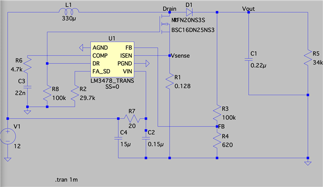
My design is an SMPS boos converter, with the following specs.
  • VIn = 12V
  • Vout = 200V
  • Iout = 6-8mA
  • Switching freq = 500KHz
And the design I came up with using an LM3478 controller is the one in the picture below.
My doubts are:
  • This boos converter will be used to feed a multiplexed load which consumes around 6mA. By multiplexing I mean it is gonna be disconnected so the circuit will be rapidly changing between load and no load condition. 2 extra mA are consumed by biasing the feedback tension divider. The matter is that the load is gonna be multiplexed at a 30-40KHz frequency (more or less). So long I made the design thinking in the 6mA load, but I am not sure if I should have considered in some way the multiplexing effect. Can I assume that the output voltage will be properly regulated without problem despite changing the load condition periodically?
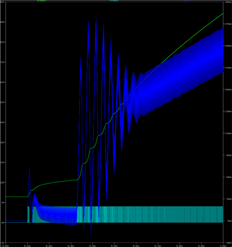
  • I tried to simulate the circuir but there is something strange with the inductor current at the beginning. The picture below shows the waveform I refer to. The dark blue waveform is the inductor current. As you can see, despite the sae-tooth shape, there is a much lower frequency oscillation at the beginning which seems to perfectly coincide with Vout derivate (light green waveform). Although I am not worried about because the peak current in steady state is slightly higher than the one in the oscillation, I have not been able to found why this happens. Could you please help me to find out why is this happening and to solve any problem in case there is one? 
  • I would also like some advice for the compensation network. I think it is good enough like this but I am not sure.
  • Finally I would love to receive some general feedback of the overall design if possible. Maybe I could add some Bypass capacitor at the output? Change Vin network value or add more bypass capacitors?

He also sent another email below.

I have been trying to simulate a design based on PMP20183B but I am a bit confused.
First of all it seems to operate in DCM and not in CCM, despite i don’t think this would be a problem for my requirements. 
Moreover, inductor current simulations results in: 

Which honestly, does not look really good. 
I have a couple of questions regarding your reference design.
Would it be possible to adapt it to work in CCM? Do you recommend me DCM over CCM? I have been trying, keeping switching frequency at 100KHz but I end up with really high inductor values (around 1mH). Do you strongly recommend me to go for 100KHz or is 500KHz good enough? I assume the main benefit of reducing the switching frequency is to reduce switching losses, but I don’t know if it really pays off in this case. Your advise on it would be great. Not only this but I haven’t been capable of adjusting ISense network for the loop to be stable… I have followed the instructions in the datasheet but I can’t come with a value that ensures stability. Only thing I manage to achieve some stability is
from LM3478 datasheet.
Any help on this or the other design I sent you a couple days ago will be appreciated. I can resend you the other design if necessary.
One last thing I would like to ask is about the output stage (I don’t really know if it is called like this). In the design you referenced there are multiple diodes and capacitors. Could you briefly explain why? Moreover, in evaluation boards design there is not just one capacitor but more than one. Is this to reduces ESR? which are the guidelines to decide how many capacitors does an application need? And its values?
Again, thank you very much for your time, patience and help. I really appreciate that.

Regards,

Danilo

  • Hi Danilo,

    Thank you for using E2E forums, there is so much to unpack here I will first answer the reviewing of the design and we can see if that answers other of your questions. First look of the design and the inductor value and the design specs it seems ok to me, although I would suggest using a lot more capacitances in the input and output you can check out the application section of the datasheet page 16 https://www.ti.com/lit/ds/symlink/lm3478.pdf?ts=1675937249566&ref_url=https%253A%252F%252Fwww.ti.com%252Fproduct%252FLM3478 there you can go through the step by step how to design the Boost converter using LM3478. 

    As for the compensation I would suggest this app note https://www.ti.com/lit/an/snva067d/snva067d.pdf?ts=1675937359578&ref_url=https%253A%252F%252Fwww.google.com%252F it explains specifically how to design the compensation circuit for this device.

    Hope this helps.

    BR,

    Haroon

  • Hi Danilo,

    One small correction after checking with my colleagues it has come to my attention that the duty cycle of the device in your proposed design will be outside what the device can handle, converting 12 to 200V almost 16 times seems improbable. I would also suggest to look into the Flyback instead of normal boost.

    Hope this helps.

    BR,

    Haroon

  • Hi Haroon,

    Thank you for your response. I suggested the PMP20183 9V-15V Input Voltage Boost Converter (200V@10mA) Reference Design which seems to meet his requirements. It has a voltage trippler to boost the voltage to 200V. Is it suitable for his application based on the condition mentioned above?

    "This boost converter will be used to feed a multiplexed load which consumes around 6mA. By multiplexing I mean it is gonna be disconnected so the circuit will be rapidly changing between load and no load condition. 2 extra mA are consumed by biasing the feedback tension divider. The matter is that the load is gonna be multiplexed at a 30-40KHz frequency (more or less). So long I made the design thinking in the 6mA load, but I am not sure if I should have considered in some way the multiplexing effect. Can I assume that the output voltage will be properly regulated without problem despite changing the load condition periodically?"

    Regards,

    Danilo

  • Hi Danilo,

    I see yeah the reference design seems to be similar to what you are trying to do, in that case it should be alright.

    Regarding the multiplexing, I think what you mean is sudden change of the load, so a load transient. In that case you would need to make your compensation circuit quite resilient and stable so that the load transient does not destabilizes your system. here is an interesting read on stability please give it a read https://www.ti.com/lit/an/slva381b/slva381b.pdf  and I would also suggest using https://www.ti.com/tool/POWERSTAGE-DESIGNER to check the phase margin, and Fco of your design.

    All the best and hope this answers your question.

    BR,

    Haroon