This thread has been locked.

If you have a related question, please click the "Ask a related question" button in the top right corner. The newly created question will be automatically linked to this question.

TPS7A8300: Deviation in Vref of Device

Part Number: TPS7A8300

Hi

Good Afternoon

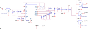
I have used the device TPS7A8300 in prototype purpose and it has worked perfectly  . Now the design is called for production. In the single board, 5 devices are called. The issue what I am facing is deviation in Vref voltage of all the 5 devices. Instead of 0.8V , its coming 0.5V. But the same design has worked.

What could be the issue. Is it the device issue ?

Regards

Vikas Kumar

  • Hi Vikas,

    Is it possible for you to share schematics of the devices? The fact that all devices are showing the same issue indicates that there is something on the board that is causing it. 

    Also, what is the input/output voltages, and expected load current?

    Thanks,

    Nick

  • Hi Vikas,

    Does the issue show up during startup or does it happen after some time being powered on? Have you captured any waveforms showing this behavior? Startup and shutdown waveforms would be helpful.

    Thanks,

    Nick

  • Hi Nick

    I am attaching the schematic.

    Input voltage is 5V and output voltages are 3.3V and 1.8V. Current is lesser than 1A.

  • Nick

    This issue is there till the board is powered on. I was using the multimeter to check the Vref voltages.

    Based on the other post, I felt there could be some issue with capacitor values, so in my prototype board, I removed all the capacitors to check its behavior, But the VREF was still 0.79 to 0.8 Volts.

    Do you want me to check in other mode of device ?

  • Hi Vikas,

    I'm a little confused by what you said. You said that after removing the capacitors, the VREF was 0.79V to 0.8V, which is what it should be. It seems to me that this solved the issue. Which capacitors did you remove for this test? Other than the BIAS capacitor (which I explain in the next paragraph), I don't see an issue with the capacitors in the schematic.

    One thing I see in the schematic is that the BIAS pin does not need a capacitor to GND if BIAS is not used. It should be left floating. I don't know what the consequence is of having the capacitor there because the datasheet does not specify, but it would be good practice to do as the datasheet says. 

    Another potential concern is the thermal performance. 5V -> 1.8V @ ~1A (I don't know how much current your application actually uses but you said the load current is less than 1A) is over 3W of power dissipation, so this has the potential to be getting the device close to thermal shutdown if the layout has flaws in regards to on-board heatsinking. Can you share a screenshot of the layout near the device? 

    It would be good to measure the input and output voltage with an oscilloscope during this fault condition because there could be important details that show the behavior that a multimeter will miss.

    Regards,

    Nick

  • Hi Nick

    Sorry for the confusion.

    I have two variants of boards. One board is for prototype. And other board is production board. Layouts are same in both . Only thing, proto board was assembled 7 yrs back. And as the requirement has come recently , production team has fabricated the board again and assembled 1 set of PCB.

    What I was telling about the Vref which is 0.79 to 0.8 V, that was measured in prototype board.

    If I measure the same in production board, the voltage comes is 0.5 V.

    The difference in these two are fabrication and the components which are procured recently.

    Your commnent "Another potential concern is the thermal performance. 5V -> 1.8V @ ~1A (I don't know how much current your application actually uses but you said the load current is less than 1A) is over 3W of power dissipation, so this has the potential to be getting the device close to thermal shutdown if the layout has flaws in regards to on-board heatsinking."  , I dont think this could be the issue, as prototype has passed thermal test as well.

    I will measure the input and output in CRO and will update you on the plots.

    Regards

    Vikas

  • Hi Vikas,

    Thanks for the explanation and update, unfortunately Nick is OoO, he will respond to you when he returns on the 21st after the US holiday.

  • Hi John

    One more interesting behavior, I observed in all the devices.

    Bias capacitor is removed, Vref was coming 0.5V. I switched to the mode where we need to connect the resistors to ground to get respective voltages. The pin connecting 1.6V, when the resistor is mounted, output voltage is 1.6V+Vref, ie 2.1 V which is coming proper and stable.

    Same thing, I did for all the 5 regulators and I am able to get the required voltage even though Vref is 0.5V.

    Regards

    Vikas

  • Hi Vikas,

    Wow, that is weird. That seems to point towards the bandgap reference voltage being wrong, but with all 5 units showing this same behavior it seems unlikely at the same time. 

    Where are you measuring VREF? At FB or NR/SS? Have you tried removing C_NR/SS and tested? It's unlikely but I wonder if there's a lot of leakage that is throwing off the reference voltage. 

    Where does the 5V come from? Have you tried powering the 5V externally with a bench supply? 

    Are there any differences in the prototype and production boards? It seems weird that all 5 production boards are failing when it works fine on the proto board.

    Regards,

    Nick

  • Hi Nick

    I tried removing the capacitors , but couldn’t see any difference.

    I am measuring the Vref at Vb pin only . Currently, I am giving the power supply through R&S source only . 

    What exactly you mean by bandgap reference voltage being wrong ? I could not understand. The only difference between proto snd production board is procurement of devices. 

    And strange thing is , still it is able to satisfy all the requirements of power supply , I am able to load all the DDS and PLL chips with these .

    Shall I proceed like this !

    Regards 

    Vikas 

  • Hi Vikas,

    I should have realized sooner, but the TPS7A8301A has a 0.5V reference voltage. Can you check which devices you have populated on the boards? 

    Regards,

    Nick

  • Hi Nick

    As per the vendor , he claims he dispatched the correct part . But when I see the marking , it differs from my proto . Based on the marking , can we figure out ?

    As no where the actual part number gets printed.

    Regards

    Vikas 

  • Hi Vikas,

    Yes we should be able to determine which device it is based on the device markings. Can you tell me what is printed on top of the package? Or a picture of the top is fine as well.

    Regards,

    Nick

  • Sorry

    The PCB was not available with me , so I could not update the marking.

    I checked , the marking on top is " SBR-TI8BI AP54-G4"

    Can you confirm , whether its required device.

    Regards

    Vikas Kumar

  • Hi Vikas,

    That is the marking on the package of the IC? It does not look like I would expect for either of these devices.

    Regards,

    Nick

  • Nick , I will upload the photo Tomo morning.

    Regards 

    Vikas 

  • Hi Vikas,

    Sounds good. I will wait for that.

    Regards,

    Nick