This thread has been locked.

If you have a related question, please click the "Ask a related question" button in the top right corner. The newly created question will be automatically linked to this question.

TPS7A20: Optimal value for output capacitor

Part Number: TPS7A20
Other Parts Discussed in Thread: TPS7A94, TPS7A21, TPS7A57

Thank you for your help.

I am currently thinking of using TPS7A2033PDQNR to generate 3.3V.

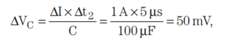
The recommended capacitance range in the specifications is 1uF-200uF, but we are considering how much capacitance to use in our actual application.

We would like to keep the load output current variation to a maximum of 150mA and the voltage variation within 0.8057mV. This is because one of the 3.3V power supply loads is using an AD converter, which is converting at

3.3V, 12bit.

For the above application, what capacitance value should I set for the capacitor?

Also, in determining the capacitance value, could you please provide some kind of calculation formula?

In addition, please tell us if there is anything we should be careful about the capacitance of the input capacitor when using an output capacitor with a large capacitance.

Thank you in advance.

  • Hello, 

    Thank you for reaching out and sharing this information. 

    Is the concern related to stability for the TPS7A20? 

    If so, staying within the recommended range should be sufficient. There is section 8.2 Typical Application in our DS that shows an example using Cin=1uF and Cout=1uF with Iout=200mA

    This used to be a bigger concern with older devices compared to modern LDOs like the TPS7A20.

    You can refer to the following app notes: Stability analysis of low-dropout linear regulators with a PMOS pass element (ti.com) and ESR, Stability, and the LDO Regulator (Rev. A) (ti.com)

    Nowadays, selecting a capacitor that meets the data sheet requirements should be sufficient for stability, therefore, looking into the impedance curve and capacitance derating is important, therefore is no need to calculate a capacitance. 

    If inrush current is the concern, here are some recommendations to help counteract the inrush current: 

    • If you are enabling the device long after the input voltage is present, then increasing Cin will help lower the initial surge of current.
    • If the device enable is tied directly to the input pin, then you will look at what is powering the linear regulator to reduce the inrush.
      • In this scenario, slowing down the rise time of the power source to the linear regulator will lower the inrush current.

    One should consider inrush current for the input and output capacitance combination, other than this, it is good analog design to place an input capacitor to counteract any reactive source and to help improve transient performance. 

    Best,

    Edgar Acosta

  • Thank you for your response.
    Please allow me to ask an additional question as I have many unclear points due to my limited design experience and knowledge.

    Is it correct to say that even with the minimum output capacitor value of 1uF listed in the datasheet, the output voltage fluctuation can be suppressed to less than 1mV for an output current fluctuation of 150mA?
    For reference, I checked the graph of load response characteristics under the conditions of Cout = 1uF and Iout = 0mAt to 300mA in "6.7 Typical Characteristics" and found that the voltage fluctuated by about 190mV.

    We are using a CMOS sensor as the load and would like to keep the voltage fluctuation to 0.8057mV, which is quite small.
    However, we have a restriction that the component mounting surface is narrow and the chip size of the capacitor must be small.

    Thank you in advance.

  • Hello, 

    Thank you for sharing more details. You are referring to a Load Transient event going from 0-150mA. 

    Is it correct to say that even with the minimum output capacitor value of 1uF listed in the datasheet, the output voltage fluctuation can be suppressed to less than 1mV for an output current fluctuation of 150mA?

    Unfortunately, no. As already noticed, going from 0-300mA  provides an undershoot of ~190mV and an overshoot of ~0.7mV. 

    The 0.8057mV is a very specific and, very challenging to be honest. The accuracy of the device also has to be considered.

    There are several factors that impact the transient performance, which means that it is a combination of different things, some of them being Load, Load Step, Slew rate, Capacitance, ESR, ESL, and the Bandwidth of the LDO. PCB parasitics will also impact this transient performance. 

    Here is an app note that talks about this: Understanding the load-transient response of LDOs (ti.com)

    By following the app note and using the Output Accuracy plot (Figure 6-13) Vout already could shift to ~3.2835V at Tj=125C and 150mA, that is ~16.5mV. 

    Now let's just assume that the 3.3V doesn't change at all, then we need a 3.2992V rail. 

    With this and assuming that the rise time for the current is 1us then you would need an ESL of~5.3713nH. 

    Then, using the 2us response time from Figure 6-55, (assuming that this will not change), using the maximum capacitance of 200uF, then the droop associated with the capacitor is ~3.7mV. 

    This already exceeds the allowable drop of 0.8057mV. 

    Meeting this 0.8mV limit is a big challenge with any type supply. 

    I understand that space is also a constraint, however, perhaps TPS7A94 and/or TPS7A57 might be of interest. And staying on the space constraint, TPS7A21. 

    These are high performance LDO's and might be an overkill for the 150mA, and might not be able to meet the sub 1mV, but it would be worth looking into. 

    Best, 

    Edgar Acosta

  • Thank you for your reply.
    ``Then, using the 2us response time from Figure 6-55, (assuming that this will not change), using the maximum capacitance of 200uF, then the droop associated with the capacitor is ~3.7mV.
    I have a question about the calculation above.
    According to the application note "Understanding the load-transient response of LDOs (ti.com)", the voltage drop due to the capacitor can be obtained by the following formula.


    If the output capacitor is 200uF, ΔI = 150mA, and the LDO response speed is 2us, isn't the voltage drop 1.5mV?
    What kind of calculation did 3.7mV come out?
    I apologize for the inconvenience, but please let me know

  • Hello, 

    My apologies, you are correct, I was looking at another value when I did the calculation. It is 1.5mV, yet this is still exceeding the required spec. 

    Also, this doesn't take into account Load regulation + Vout accuracy, parasitics, and it is assuming that the response time of the LDO will remain the same, yet this varies. 

    I can go ahead and take a bench measurement with the given conditions just to have actual data to show what the expected value could be. 

    Best, 

    Edgar Acosta