This thread has been locked.

If you have a related question, please click the "Ask a related question" button in the top right corner. The newly created question will be automatically linked to this question.

TPS1211-Q1: Gate-Source clamp needed?

Part Number: TPS1211-Q1

Hello team,

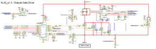
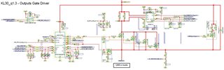
Does the TPS1211-Q1 integrate any kind of gate-source clamping?

Is it recommended to be added externally otherwise?

Thanks and best regards,

Juan.


  • Hi Juan,

    The driver limits the BST-SRC voltage so it indirectly clamps the max voltage between gate-source. There is no need to add external clamping circuits.

    Best Regards,

    Rakesh

  •  Thank you so much for your reply.

    We have also another question regarding the differences btw TPS1211 and TPS1213.

    It seems TPS1211 is a stronger driver with 4A pullup and pulldown capability. 
    But, for TPS1213 this current is reduced to 1.69A

    How it affects to drive the number of MOSFETs that are in parallel?


    For TPS1211 we have 5 B2B MOSFETs (in total 10 MOSFETs). Is TPS1213 still able to drive 10 MOSFETs? 


    Thanks in advanced,

    Navid

  • Hi Navid,

    As the GATE drive strength reduces, the turn-on time increases but it would be able to drive 10 MOSFETs

    We can calculate as turn-on time (miller region is important, where VDS discharges) as follows

    ton = 10*Cgd*Vin/ gate drive current.

    Unless, we do continuous switching, I don't see any concern in driving 10 MOSFETs.

    Best Regards,

    Rakesh

  • Hi again Rakesh,

    Can I ask what is the main limitation regarding the number of MOSFETs that TPS1213 can drive?
    Currently we have 5 B2B MOSFETs (in total 10 MOS), and due to thermal issues it is requested if it is possible to increase the MOS to 6 B2B (total 12 MOS) or 7 B2B (total 14 MOS).
    But I can not find any restriction about the number of mosfet that TPS1213 can drive in datasheet. Just increasing the CBST is enough?
    (Qtot of our selected MOS is 180nC).

    Thanks in advance for your consideration,

    Navid

  • Hi Navid,

    Sizing the CBST capacitor would be sufficient to drive more number of MOSFETs. I don't see any concern in using 14 MOSFETs at PU/PD

    Best Regards,

    Rakesh

  • Hi Rakesh,

    First, thanks for your reply,

    I came up with other issue regarding avalanche mode of Mosfet for TPS1213 applications. As you know, when the Mosfet will switch off, due to inductive load characteristics and wire harness inductance, clamp circuit is required to limit Mosfet Vds and keep the junction temperature of Mosfet inside the safe operating area. However for high current load (160-250A) I couldn´t find a proper TVS and several parallel TVS is required that cause some other issues. 

    I did a simulation and the preliminary results shows that if we put a TVS (Ex. 24V) between drain of N-Mosfet and G1PD (tha is also connected to G1PU) it can clamp the Vds voltage with low power dissipation in TVS.
    I wanted to ask if any analysis is done about this for TPS1213? 
    Or Avalanche mode is considered in TPS1213 to be protected by some external circuit?   

    Thanks in advance,

    Navid

  • Hi Navid,

    Sorry, I clicked it as resolved by mistake. We have not done such analysis.

    Can you please share the input and output inductance details in your system to check. What is the application use case?

    Thanks 

    Rakesh

  • Hi Rakesh,

    The wire inductance for different outputs is different but roughly less than 100nH for input and 50nH for output, and load inductance 5-10uH. 
    There are several outputs with various applications like brakes (Motor + Valve), EPAS, Fused SCR.
    But, right now we are focusing on QMC load (ADAS) with 160A normal operation, 255A for 1sec, and 630A  short circuit level (Four MOSFETs are in parallel). 
    Please let me know if further information is required.

    Regards,

    Navid

  • Thanks for the information 

    I  will check and get back by end of this week.

    Best regards 

    Rakesh

  • Hi Navid,

    I see that your input and output inductances are not that much. Major part is coming from the load inductance. Have you considering any freewheeling path at the output during inductive load turn-off

    Can you share your schematic to look at

    Best regards 

    Rakesh

  • Hi Rakesh,

    Regarding input and output inductance, sorry, I made a mistake. For one of our outputs with 4m wire length the output inductance is about 6uH.   
    No we don´t have freewheeling path at output load (schematic below).
    We are thinking to use unidirectional TVS in parallel with MOSFET (also a rectifier diode in series with TVS to block the current in reverse voltage). 
    But we are not sure it can survive MOS in avalanche mode? Maybe several TVS should be used in parallel. 


    PS: Using TVS between drain and G1PD IC pin cannot be a case to tackle this issue?

    Any issue please let me know,

    Thanks,

    Navid

  • Hi Navid,

    Can you share higher resolution image. 

    What is the purpose of FET between output and SRC?

    Best regards 

    Rakesh

  • Hi Rakesh,

    Please check link below for a probable higher resolution image (I couldn´t use the insert button to provide a high resolution image, I don´t know how I can send you a better quality pic). 
    The purpose of P-FET mosfet is to make the main mosfet enable in reverse voltage (as it proposed by you in a meeting we had some weeks ago). 

    /resized-image/__size/320x240/__key/communityserver-discussions-components-files/196/QMC.JPG 

    Regards,

    Navid

  • Hi Navid,

    In case of parallel MOSFET configuration, the Vds clamp solution of placing TVS diode between Drain and GATE of the MOSFET may not be a good option. The mismatch between the parallel MOSFETs will lead to unequal power stress and can damage the MOSFETs. 

    Using TVS diodes 5.0SMD type at the input and schottky diode (similar to SBR10U45SP5-13) at the output would be better options.

    Best regards 

    Rakesh