I am debugging and testing a power supply board, this power supply board has two LM5116 DC-DC controller to generate two DC power supply, the original design engineer has left I have to take the ownership.
One DC-DC was designed:
The input voltage range: 42V-53V
Output voltage: 27.5V
Maximum Load 5A
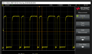
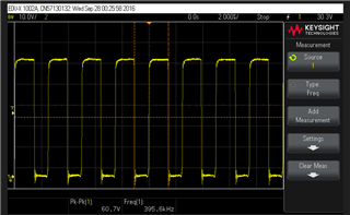
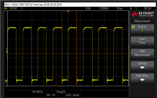
When I tested the SW signal at Pin HO, I found the SW signal waveform is not as my expected: the signal pulse width is varying as the below picture:
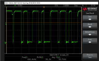
This signal waveform was captured under 0.5A current load, actually when I changed the current load from 0.5A to full load 5A, this problem is similar, the pulse width is varying.
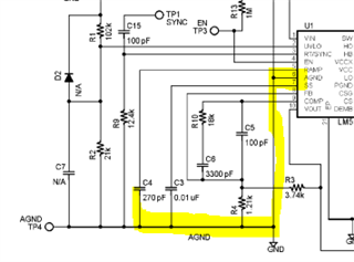
The schematic is as below:
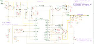
Would you give some advice what 's wrong with the design that caused SW signal pulse width is varying?
1, Inductor is 12 UH, do you think it is big enough?
2, Input/output ceramic capacitor is 2.2uf, is it big enough because I found on EVAL board, all the ceramic capacitor value are bigger than 2.2uf
3,Cramp/Rramp value are right?
4, I checked the PCB Layout and found Cramp was placed very closed to Csw, do you think Ramp signal is interfered by the Csw switching signal?
Thanks and best regards


