


Hi team,
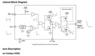
The block diagram on the datasheet may be incorrect.
According to the diagram, If the sense voltage is lower than the threshold, the comparator's output is Low, AND logic output is Low, then Pch FET is on and CT capacitor will be chaged. It means CT timer is Reset detection delay but, it should be Reset release delay.
So, the AND logic should be NAND logic. If so, the buffer after CT should be inverter.
Is my understanding correct?
If so, please update the diagram at the next datasheet update.
Regards,
