Other Parts Discussed in Thread: ISO7741
Hi experts,
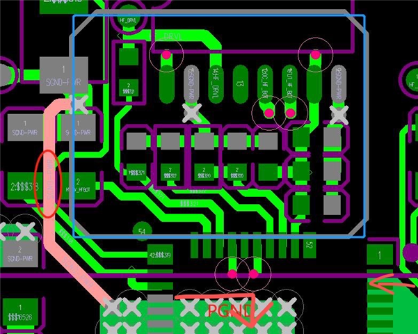
Here is my customer's LMG3522R030 PCB layout, the kelvin connection between signal ground and Source of GaN is shown in the figure below:
use a trace to connect two coppers instead of vias like the EVM.
According to the previous layout experience of Si MOS, but not sure whether it is applicable to GaN HEMT.
The blue box is signal ground shielding layer, the red circle is the trace of kelvin to the bottom GaN Source.
The top GaN too.


