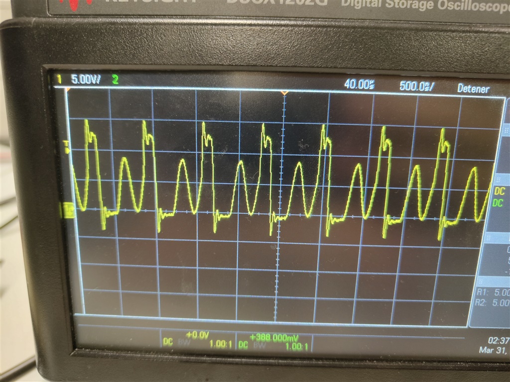
This thread has been locked.

If you have a related question, please click the "Ask a related question" button in the top right corner. The newly created question will be automatically linked to this question.

BQ25895: It don't charge

Part Number: BQ25895

Hi, 

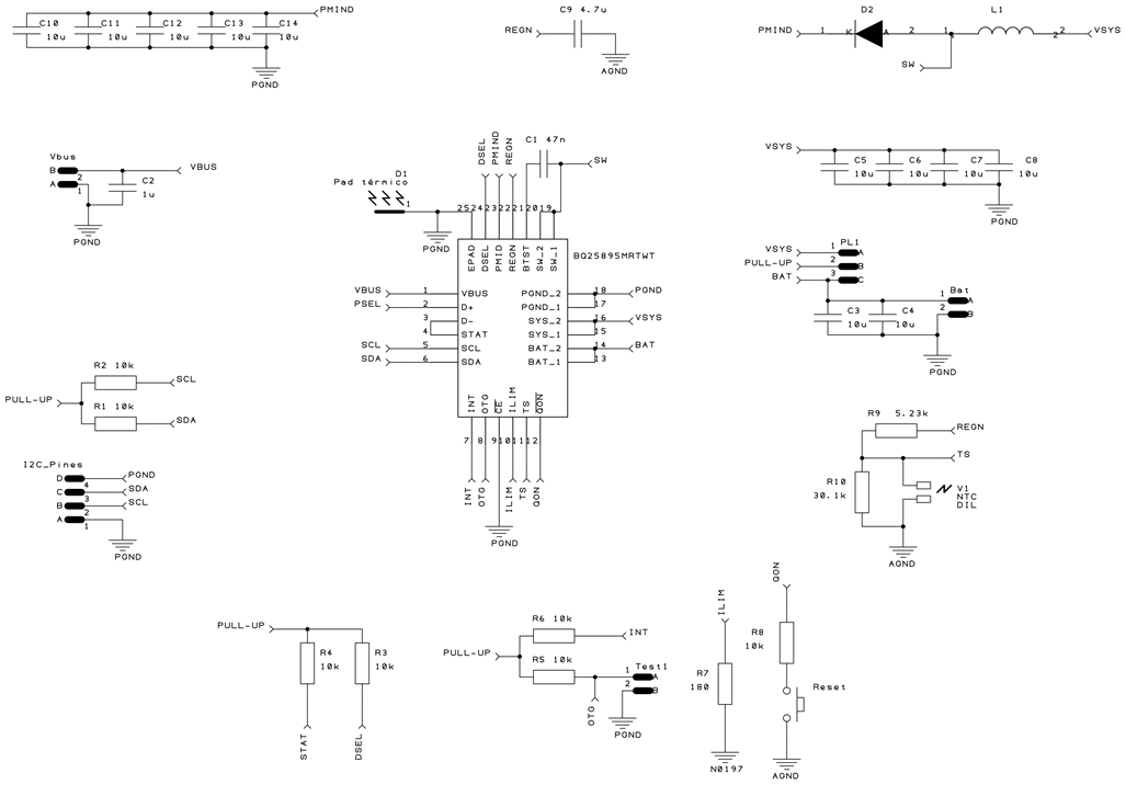
I have made a custom pcb with the bq25895 based on https://www.ti.com/tool/BQ25895EVM-664.

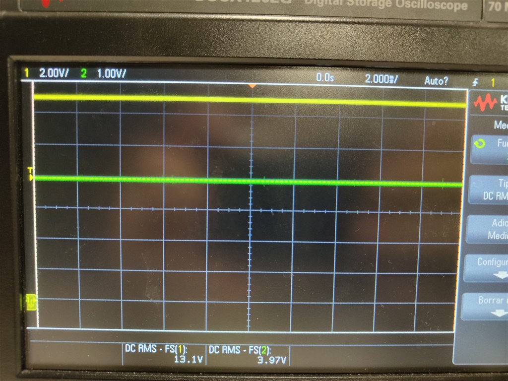
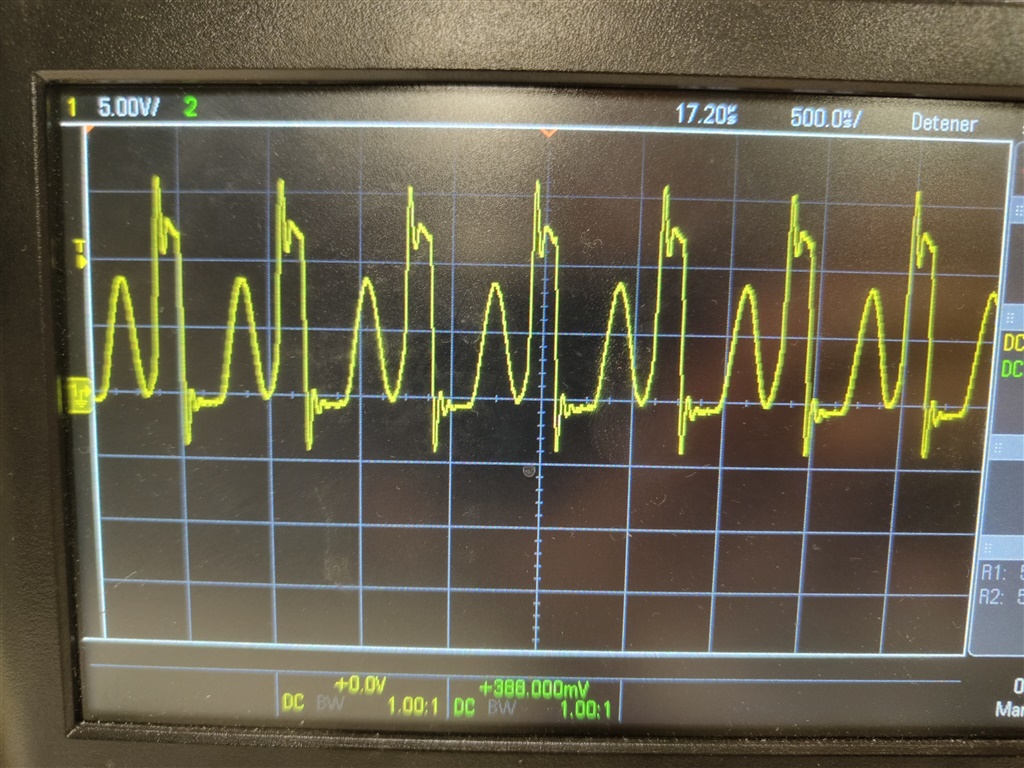
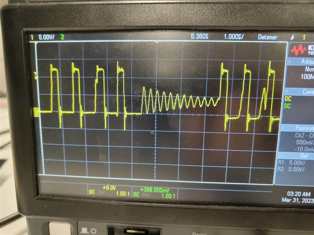
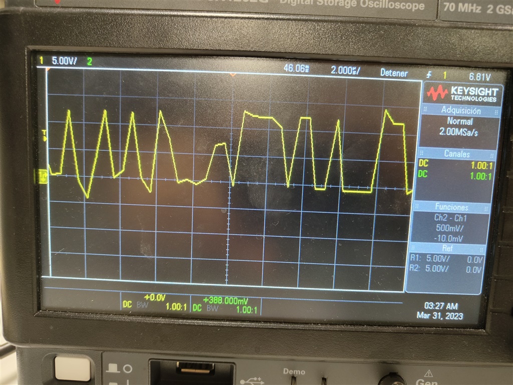
I have a 12V power supply connected to Vbus. I know I haven't shorted the D+ and D- pins. Ilim is configured with a resistance equivalent to 133 ohms.

I have read the FAQ file (Link) and I haven't found the error.

At this moment I don't have any load connected to Pmind or Vsys and even so it doesn't charge the battery.

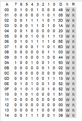
Reading the logs I get these results:

Read REG 0x00: 0 1 0 0 1 0 0 0
Read REG 0x01: 0 0 0 0 0 1 0 1
Read REG 0x02: 0 0 1 1 1 1 0 1
Read REG 0x03: 0 0 1 1 1 0 1 0
Read REG 0x04: 0 0 1 0 0 0 0 0
Read REG 0x05: 0 0 0 1 0 0 1 1
Read REG 0x06: 0 1 0 1 1 1 1 0
Read REG 0x07: 1 0 0 1 1 1 0 1
Read REG 0x08: 0 0 0 0 0 0 1 1
Read REG 0x09: 0 1 0 0 0 1 0 0
Read REG 0x0A: 1 0 0 1 0 0 1 1
Read REG 0x0B: 1 0 1 0 0 1 1 1
Read REG 0x0C: 1 0 0 0 0 0 0 0
Read REG 0x0D: 0 1 1 0 0 0 1 0
Read REG 0x0E: 0 0 0 0 0 0 0 0
Read REG 0x0F: 0 0 0 0 0 0 0 0
Read REG 0x10: 0 0 0 0 0 0 0 0
Read REG 0x11: 1 1 1 0 1 1 0 0
Read REG 0x12: 0 0 0 0 0 0 0 0
Read REG 0x13: 0 0 0 0 1 0 0 0
Read REG 0x14: 0 0 1 1 1 0 0 1

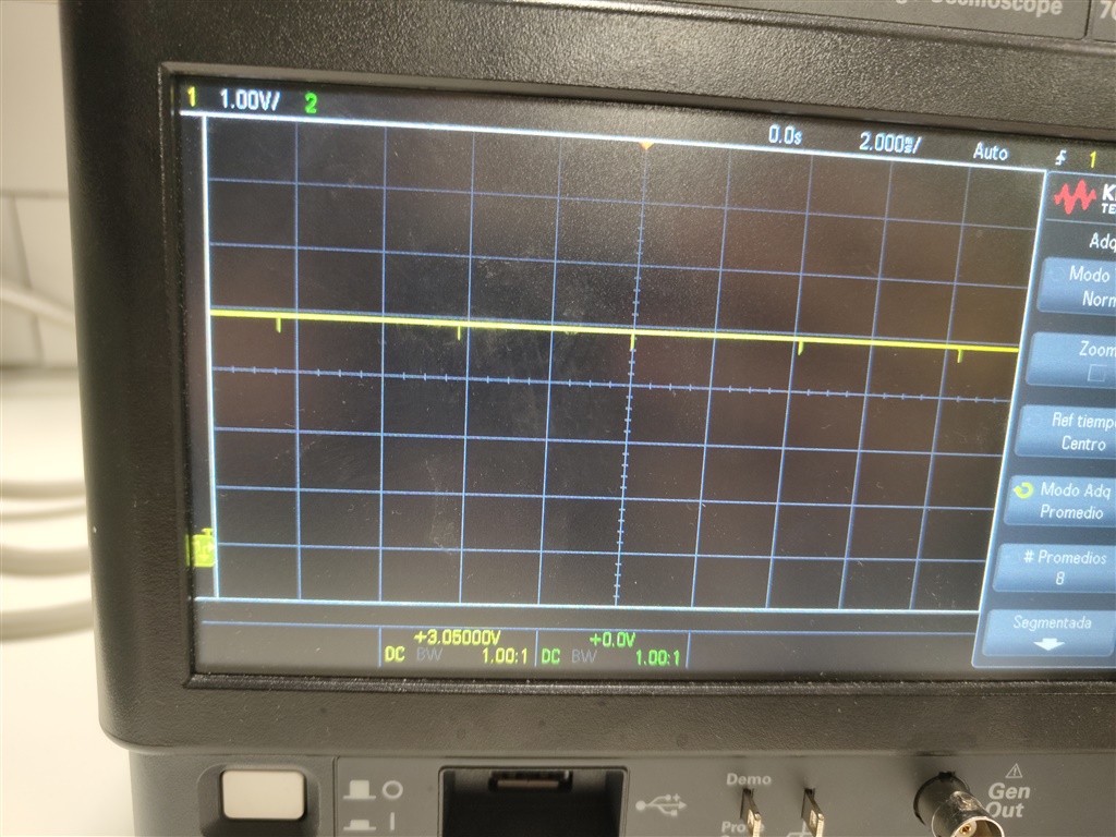
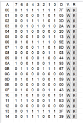
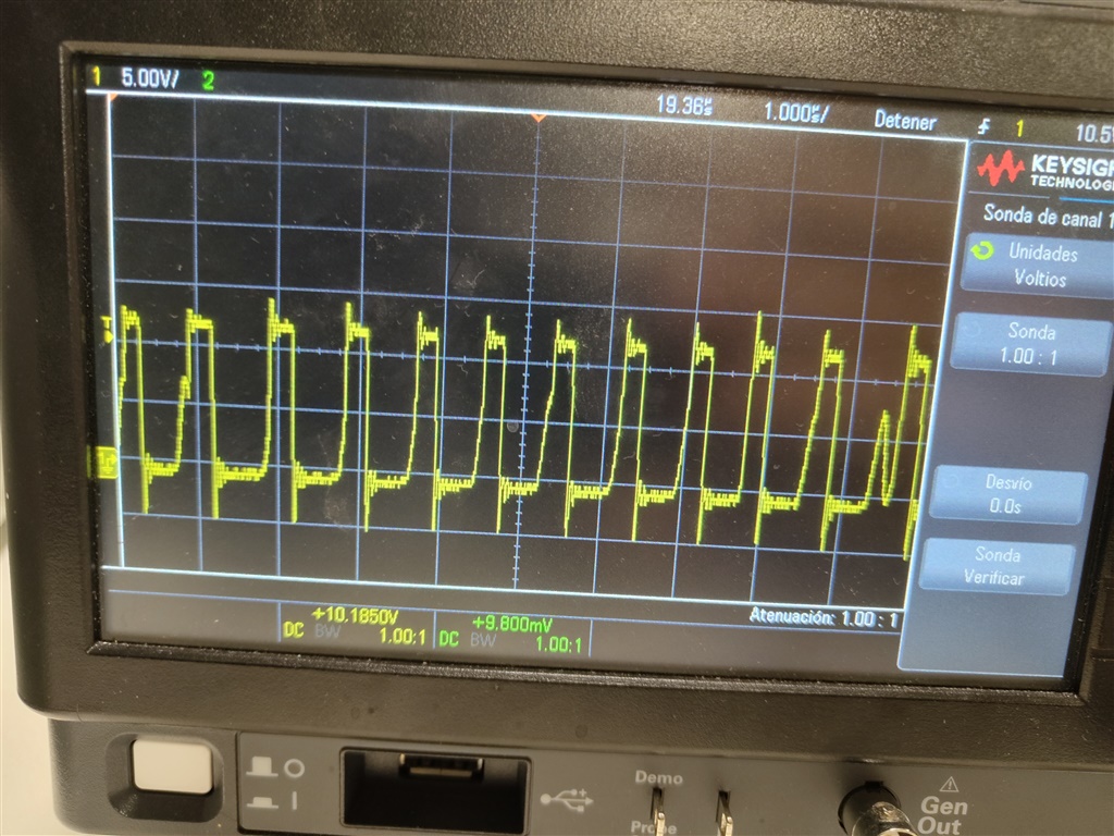
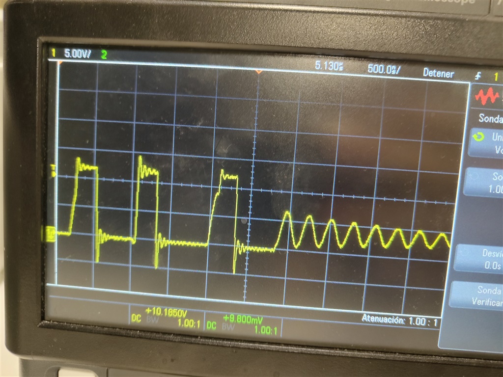
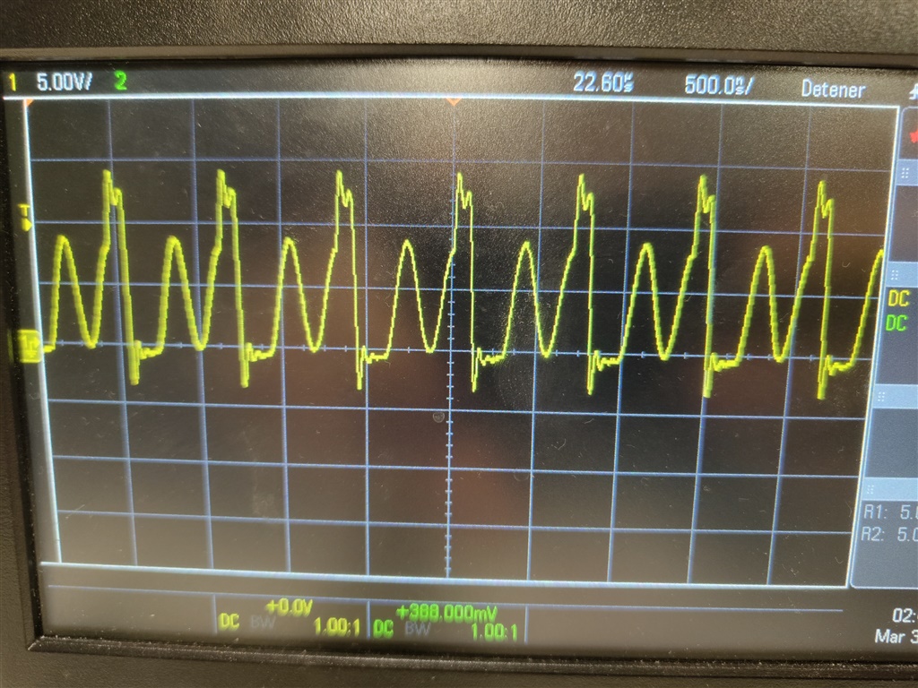
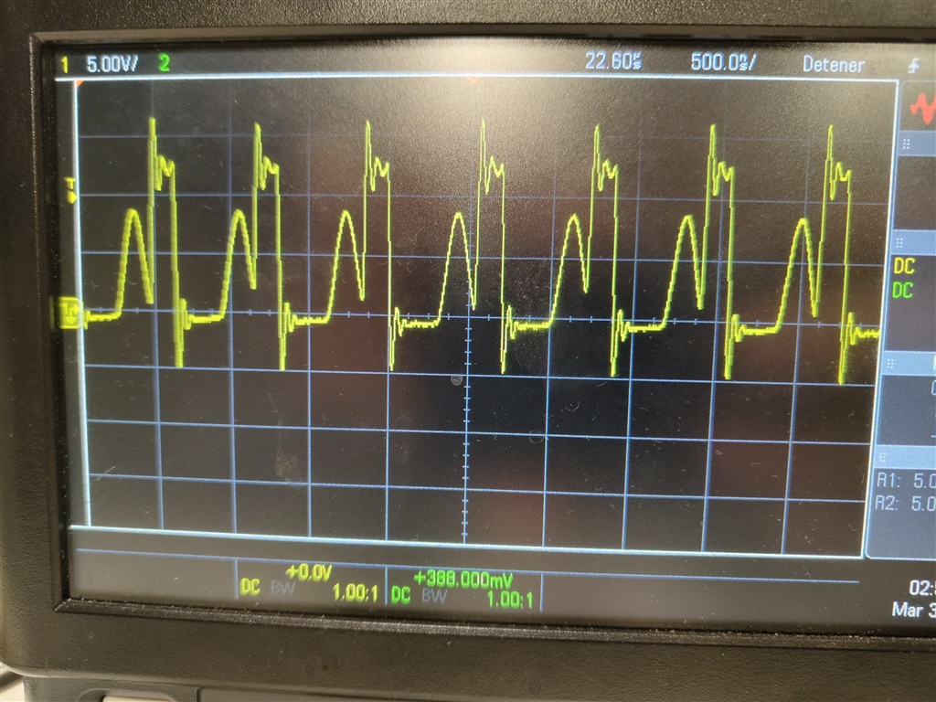
If I connect a 15 ohm load on the output of Pmid, reading the logs I get these results:

Read REG 0x00: 0 1 0 0 1 0 0 0
Read REG 0x01: 0 0 0 0 0 1 0 1
Read REG 0x02: 0 0 1 1 1 1 0 1
Read REG 0x03: 0 0 1 1 1 0 1 0
Read REG 0x04: 0 0 1 0 0 0 0 0
Read REG 0x05: 0 0 0 1 0 0 1 1
Read REG 0x06: 0 1 0 1 1 1 1 0
Read REG 0x07: 1 0 0 1 1 1 0 1
Read REG 0x08: 0 0 0 0 0 0 1 1
Read REG 0x09: 0 1 0 0 0 1 0 0
Read REG 0x0A: 1 0 0 1 0 0 1 1
Read REG 0x0B: 1 0 1 0 0 1 1 0
Read REG 0x0C: 1 0 0 0 0 0 0 0
Read REG 0x0D: 0 1 1 0 0 0 1 0
Read REG 0x0E: 0 0 0 0 0 0 0 0
Read REG 0x0F: 0 0 0 0 0 0 0 0
Read REG 0x10: 0 0 0 0 0 0 0 0
Read REG 0x11: 1 1 1 0 1 1 0 0
Read REG 0x12: 0 0 0 0 0 0 0 0
Read REG 0x13: 0 0 0 0 1 0 0 0
Read REG 0x14: 0 0 1 1 1 0 0 1

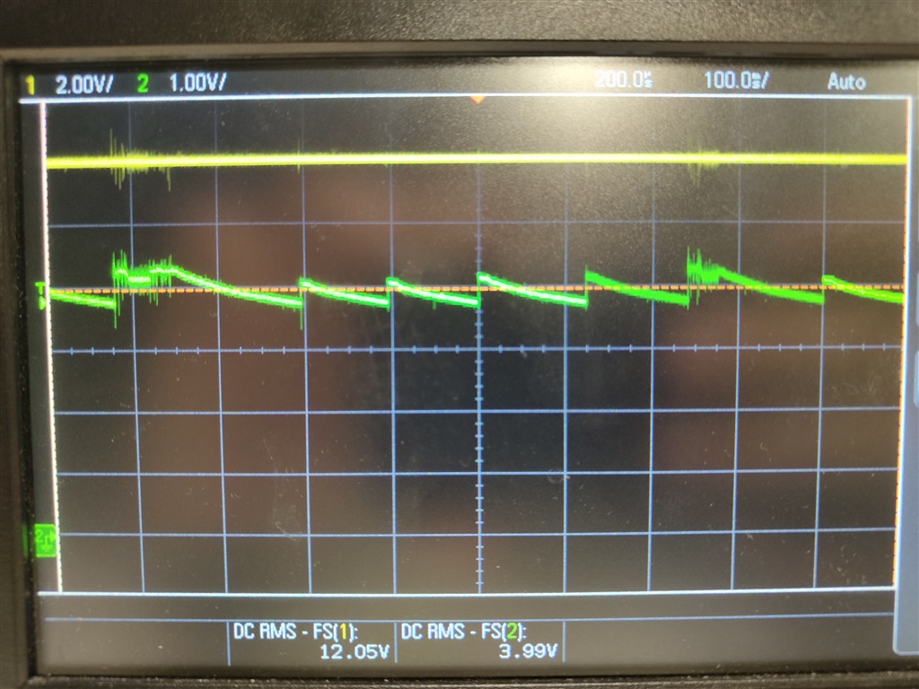
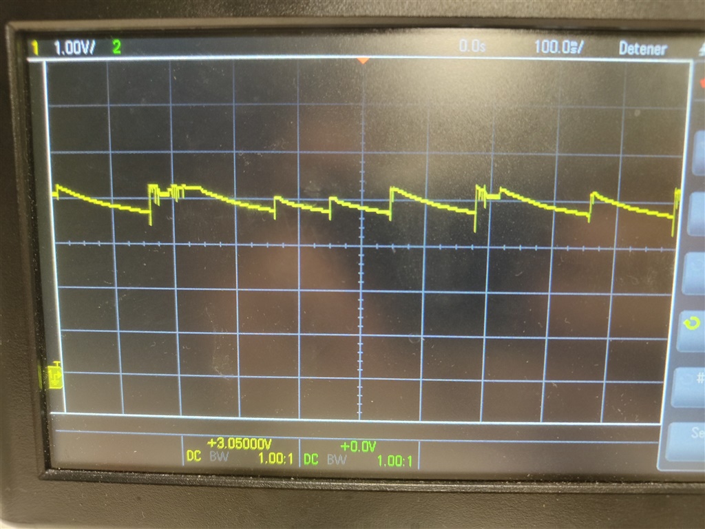
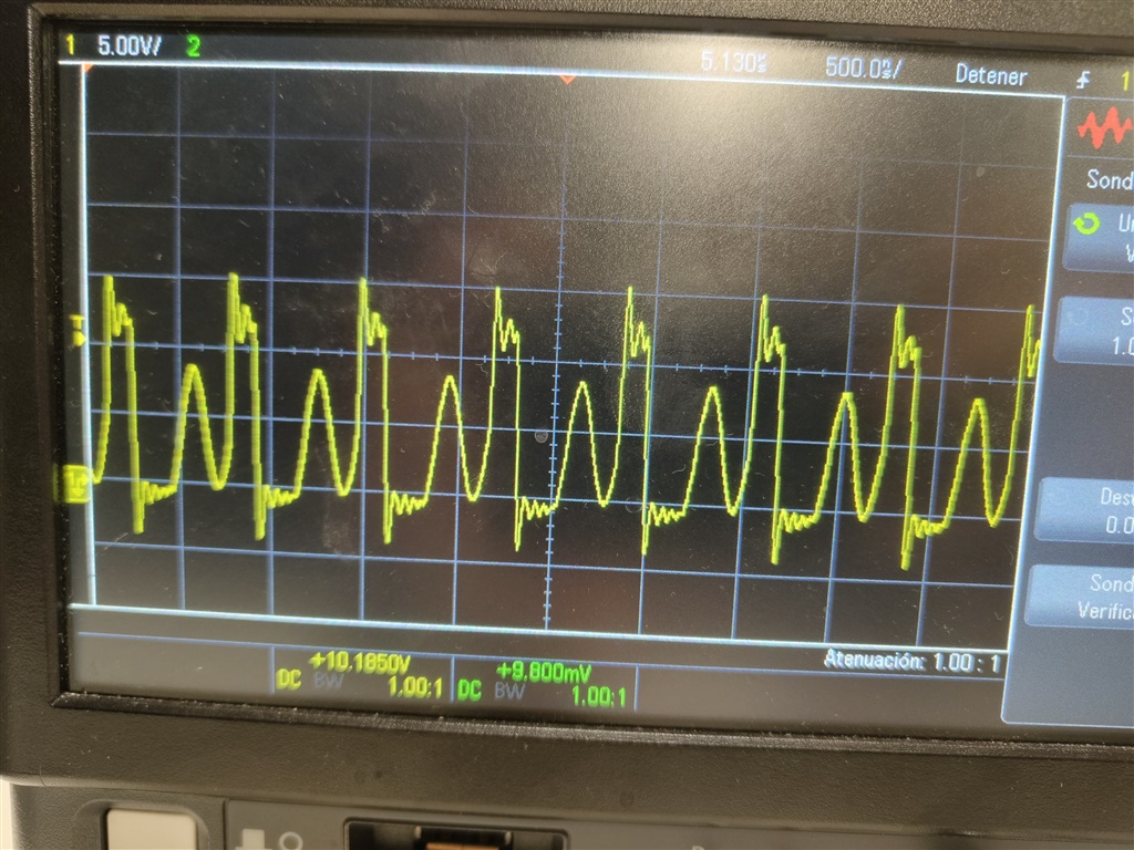
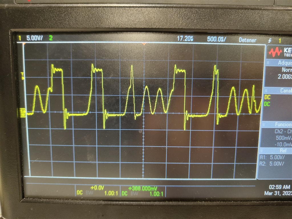
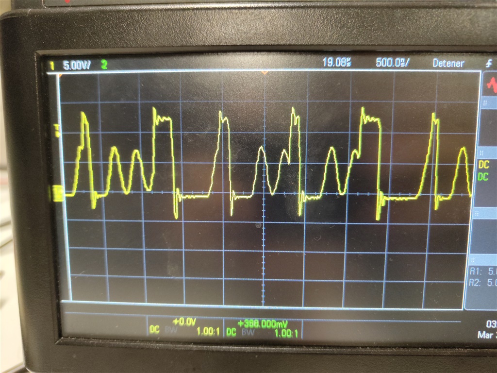
If I connect a 15 ohm load on the output of Vsys, reading the logs I get these results:

Read REG 0x00: 0 1 0 0 1 0 0 0
Read REG 0x01: 0 0 0 0 0 1 0 1
Read REG 0x02: 0 0 1 1 1 1 0 1
Read REG 0x03: 0 0 1 1 1 0 1 0
Read REG 0x04: 0 0 1 0 0 0 0 0
Read REG 0x05: 0 0 0 1 0 0 1 1
Read REG 0x06: 0 1 0 1 1 1 1 0
Read REG 0x07: 1 0 0 1 1 1 0 1
Read REG 0x08: 0 0 0 0 0 0 1 1
Read REG 0x09: 0 1 1 0 0 1 0 0
Read REG 0x0A: 1 0 0 1 0 0 1 1
Read REG 0x0B: 1 0 1 0 0 1 1 0
Read REG 0x0C: 1 0 0 0 0 0 0 0
Read REG 0x0D: 0 1 1 0 0 0 1 0
Read REG 0x0E: 0 0 0 0 0 0 0 0
Read REG 0x0F: 0 0 0 0 0 0 0 0
Read REG 0x10: 1 1 1 1 1 1 1 1
Read REG 0x11: 1 1 1 0 1 1 0 0
Read REG 0x12: 0 0 0 0 0 0 0 0
Read REG 0x13: 0 1 0 0 0 0 1 0
Read REG 0x14: 0 0 1 1 1 0 0 1

How can I fix this error?

Raúl

  • Hi Raul, 

    Thank you for reaching out via E2E and providing your schematic and register logs.

    Please see my comments below. 

    -Are any of the components shown in the schematic not placed on your PCB? For example, there should not be two inductors connected to SW. Please help to provide an updated schematic which shows passive components populated on your PCB. 

    -Looking at all 3 register logs it appears the charge state (REG0B bits 4-3) always reads 00b = not charging. Can you confirm that you are driving /CE pin low to enable charging. 

    -The 3rd register log with a load on SYS indicates that the BATFET has been turned off (REG09 bit 5). You will not be able to charge the battery with BATFET_DIS = 1. Please make sure BATFET_DIS = 0 before you attempt to charge the battery. You may need to check your test setup if BATFET_DIS is being automatically set = 1 due battery protection feature. 

    To continue with debug I recommend to continue testing with no load at PMID or SYS. Connect the battery first then VBUS and ensure /CE is low. At that point the register log should show an error if charge is not able to be started. 

    Regards,

    Garrett 

  • Hi,
    Thank you for answering so quickly.
    1. Regarding the components, I followed the reference PCB schematic. On this PCB there are some components where it says DNP, I understood that these were optional and I installed them. The only one that I did not install is D3, it connects pin 22 with 21.
    2. I already checked this, just like on the reference board I put the /CE pin connected to the pull-up with a 10K ohm resistor. When I try to charge the battery, 2V circulates on that pin. If I use the jumper to connect it to GND it still doesn't load.
    3. As you can see, the design is almost identical to that of the reference pcb, after reviewing I have not found any differences.

    As you requested I have done a test without load, connecting the /CE pin to GND, then connecting the battery and finally connecting Vbus. The results have been the following:

    Read REG 0x00: 0 1 0 0 1 0 0 0
    Read REG 0x01: 0 0 0 0 0 1 0 1
    Read REG 0x02: 0 0 1 1 1 1 0 1
    Read REG 0x03: 0 0 1 1 1 0 1 0
    Read REG 0x04: 0 0 1 0 0 0 0 0
    Read REG 0x05: 0 0 0 1 0 0 1 1
    Read REG 0x06: 0 1 0 1 1 1 1 0
    Read REG 0x07: 1 0 0 1 1 1 0 1
    Read REG 0x08: 0 0 0 0 0 0 1 1
    Read REG 0x09: 0 1 0 0 0 1 0 0
    Read REG 0x0A: 1 0 0 1 0 0 1 1
    Read REG 0x0B: 1 0 1 0 0 1 1 0
    Read REG 0x0C: 1 0 0 0 0 0 0 0
    Read REG 0x0D: 0 1 0 1 0 1 1 1
    Read REG 0x0E: 0 0 0 0 0 0 0 0
    Read REG 0x0F: 0 0 0 0 0 0 0 0
    Read REG 0x10: 0 0 0 0 0 0 0 0
    Read REG 0x11: 1 1 1 0 0 0 0 1
    Read REG 0x12: 0 0 0 0 0 0 0 0
    Read REG 0x13: 0 0 0 0 1 0 0 0
    Read REG 0x14: 0 0 1 1 1 0 0 1

    Having installed all the DNP components, I have seen that two coils placed in parallel, one being 2.2 uH and the other 1.5 uH, left an equivalent of 0.89uH. According to the FAQ pdf, this would have to be between 1 uH and 2.2 uH, so I have unsoldered the 1.5 uH one. After repeating the test, the battery still did not charge and the results were as follows.

    Read REG 0x00: 0 1 0 0 1 0 0 0
    Read REG 0x01: 0 0 0 0 0 1 0 1
    Read REG 0x02: 0 0 1 1 1 1 0 1
    Read REG 0x03: 0 0 1 1 1 0 1 0
    Read REG 0x04: 0 0 1 0 0 0 0 0
    Read REG 0x05: 0 0 0 1 0 0 1 1
    Read REG 0x06: 0 1 0 1 1 1 1 0
    Read REG 0x07: 1 0 0 1 1 1 0 1
    Read REG 0x08: 0 0 0 0 0 0 1 1
    Read REG 0x09: 0 1 0 0 0 1 0 0
    Read REG 0x0A: 1 0 0 1 0 0 1 1
    Read REG 0x0B: 1 0 1 0 0 1 1 0
    Read REG 0x0C: 1 0 0 0 0 0 0 0
    Read REG 0x0D: 0 1 0 1 0 1 1 1
    Read REG 0x0E: 0 0 0 0 0 0 0 0
    Read REG 0x0F: 0 0 0 0 0 0 0 0
    Read REG 0x10: 0 0 0 0 0 0 0 0
    Read REG 0x11: 1 1 1 0 0 0 0 1
    Read REG 0x12: 0 0 0 0 0 0 0 0
    Read REG 0x13: 0 0 0 0 1 0 0 0
    Read REG 0x14: 0 0 1 1 1 0 0 1

    Any idea how to fix the problem?
    Thank you,
    Raul.

  • Hi Raul, 

    I recommend starting by removing the majority of components marked DNP on the EVM schematic that you have on the board. Capacitors marked DNP at VBUS,PMID, and BAT do not need to be removed. 

    The components populated on your board should match the TI recommendations found in the BQ25895 schematic checklist, which can be found at the FAQ you linked in your initial post.  Based on my review please remove the 10K pullup resistor at /CE (R8), D1 between GND and SW pin, and ensure the capacitance at SYS does not exceed 40 uF. 

    After removing these components please attempt to charge again. The voltage at /CE pin should = GND for charge to be enabled. If you are still seeing issues can you provide a waveform showing VBUS and VSYS. 

    Regards,

    Garrett 

  • Hi,

    have removed the DNP components and the others as you told me.

    I have done the test you asked me to do. You had not specified if the battery had to be connected, I have done both ways. always connecting /CE to GND.

    1) With battery

    Yellow - Vbus

    Green - Vsys

    The pcb is connected to a 12V and 450mA power supply. Using 3 multimeters I have measured Vbus (12.00V), Vsys (3.995V) and Vbat (3.996V). This doesn't match, the oscilloscope marks Vbus at about 4V and Vsys at about -4V.

    Also, measuring the current of the battery, it is discharging at -0.12 mA.

    2) No battery

    Everything behaves the same, but Vsys is not that stable, it has some spikes.

    Any idea what's going on?
    Thank you,
    Raul

  • Hi Raul, 

    The multimeter measurements with the battery connected are in the range of what I would expect, but the battery should be charging. I would also double check that you are setting up your oscilloscope correctly. VBUS, VBAT, and VSYS should all be stable DC signals when a battery is connected. Do you by chance have the BQ25895EVM? Performing a test on this board would eliminate any potential issue with the PCB as the root cause. 

    What is the multimeter reading of SYS voltage when you have input at VBUS, but no battery connected? By chance does your board have a test point you can probe at the SW node? It will be helpful to confirm if the device is switching. The SW waveforms should look like figure 9-10 on page 52 of the datasheet.

    Can you also provide the register reading (in hex instead of binary if possible) of the test with VBUS and battery connected. For that register reading can you enable the ADC (REG02 bit 7 = 1) as well so the ADC output registers REG0E through REG12 are not just all zeros. 

    Regards,

    Garrett 

  • Hi,

    I don't have the BQ25895EVM PCB, but I've repeated the tests and got better results.

    1) Vbus (yellow) and Vbat connected and the measurements are included (Vsys - green):

    Vbat is 3.995V

    Register log:

    Read REG 0x00: 0 1 0 0 1 0 0 0
    Read REG 0x01: 0 0 0 0 0 1 0 1
    Read REG 0x02: 1 0 1 0 0 0 0 0
    Read REG 0x03: 0 0 1 1 1 0 1 0
    Read REG 0x04: 0 0 1 0 0 0 0 0
    Read REG 0x05: 0 0 0 1 0 0 1 1
    Read REG 0x06: 0 1 0 1 1 1 1 0
    Read REG 0x07: 1 0 0 1 1 1 0 1
    Read REG 0x08: 0 0 0 0 0 0 1 1
    Read REG 0x09: 0 1 0 0 0 1 0 0
    Read REG 0x0A: 1 0 0 1 0 0 1 1
    Read REG 0x0B: 0 0 0 0 0 1 1 1
    Read REG 0x0C: 0 0 0 0 0 0 0 0
    Read REG 0x0D: 0 1 1 0 0 0 0 1
    Read REG 0x0E: 0 0 0 0 0 0 0 0
    Read REG 0x0F: 0 0 0 0 0 0 0 0
    Read REG 0x10: 0 1 0 1 0 1 1 1
    Read REG 0x11: 1 1 1 0 1 0 1 1
    Read REG 0x12: 0 0 0 0 0 0 0 0
    Read REG 0x13: 0 0 0 0 1 0 0 0
    Read REG 0x14: 0 0 1 1 1 0 0 1

    SW signal:

    2) Vbus (yellow) connected and the measurements are included (Vsys - green):

    Register log:

    Read REG 0x00: 0 1 0 0 1 0 0 0
    Read REG 0x01: 0 0 0 0 0 1 0 1
    Read REG 0x02: 0 0 1 1 1 1 0 1
    Read REG 0x03: 0 0 1 1 1 0 1 0
    Read REG 0x04: 0 0 1 0 0 0 0 0
    Read REG 0x05: 0 0 0 1 0 0 1 1
    Read REG 0x06: 0 1 0 1 1 1 1 0
    Read REG 0x07: 1 0 0 1 1 1 0 1
    Read REG 0x08: 0 0 0 0 0 0 1 1
    Read REG 0x09: 0 1 0 0 0 1 0 0
    Read REG 0x0A: 1 0 0 1 0 0 1 1
    Read REG 0x0B: 1 0 1 0 0 1 1 0
    Read REG 0x0C: 1 0 0 0 0 0 0 0
    Read REG 0x0D: 0 1 1 0 0 0 0 1
    Read REG 0x0E: 0 0 0 0 0 0 0 0
    Read REG 0x0F: 0 0 0 0 0 0 0 0
    Read REG 0x10: 0 0 0 0 0 0 0 0
    Read REG 0x11: 1 1 1 0 1 0 1 1
    Read REG 0x12: 0 0 0 0 0 0 0 0
    Read REG 0x13: 0 0 0 0 1 0 0 0
    Read REG 0x14: 0 0 1 1 1 0 0 1

    SW signal:

    I hope it solves the confusion of the previous comment.

    But the battery continues to discharge.

    Raul.

  • Hi Raul, 

    The device continues to not work as expected. Based on the register log the device detects you input at VBUS, but does not correctly detect voltage at BAT pin or SYS pin. Not detecting the battery may be why charge does not begin. This leads me to believe there may be some issue with your board and there is a chance that caused damage to the device. 

    Can you work to replicate a couple specific tests I will outline below.

    1)Test battery only operation through the BATFET. Only connect your battery and a load at SYS. Have the load be in the range of a 500 mA current draw. Then for registers leave all registers at default values other than turning off OTG (set REG03 bit 5 = 0b) and disable watchdog timer (set REG07 bits 5:4 = 00b). Then enable the ADC (set REG02 bit 7 = 1b) and read all registers. 

    Below is expected register log when connecting VBAT = 3.95V. You should observe the battery discharge to SYS to power the load you have connected. Please provide the register log and multimeter measurements of BAT and SYS.

    2) Test SW node operation with charge disabled since you are currently unable to get battery to start charging. 

    For this test do not connect the battery. Just connect your input power supply to VBUS and a load in the range of 500mA to 1A at SYS. Leave all registers at default values other than disabling charge (set REG03 bit 4 = 0b) and disabling watchdog timer (set REG07 bits 5:4 = 00b).

    Below is example register log. Depending on your adapter type the input current & voltage limits may be different, which is okay. Please enable the ADC to see if BQ25895 correctly detects voltage at VBUS and SYS. 

    Please provide your register log, multimeter measurements at VBUS and SYS and an oscilloscope capture of SW node. I have provided a capture of what SW node should look like as reference. 

    Best Regards,

    Garrett

  • 1) Log:

    Read REG 0x00: 0 1 0 0 1 0 0 0
    Read REG 0x01: 0 0 0 0 0 1 0 1
    Read REG 0x02: 0 0 1 1 1 1 0 1
    Read REG 0x03: 0 0 0 1 1 0 1 0
    Read REG 0x04: 0 0 1 0 0 0 0 0
    Read REG 0x05: 0 0 0 1 0 0 1 1
    Read REG 0x06: 0 1 0 1 1 1 1 0
    Read REG 0x07: 1 0 0 0 1 1 0 0
    Read REG 0x08: 0 0 0 0 0 0 1 1
    Read REG 0x09: 0 1 0 0 0 1 0 0
    Read REG 0x0A: 1 0 0 1 0 0 1 1
    Read REG 0x0B: 0 0 0 0 0 0 1 0
    Read REG 0x0C: 1 0 0 0 0 0 0 0
    Read REG 0x0D: 0 0 0 1 0 0 1 1
    Read REG 0x0E: 0 0 0 0 0 0 0 0
    Read REG 0x0F: 0 0 0 0 0 0 0 0
    Read REG 0x10: 0 0 0 0 0 0 0 0
    Read REG 0x11: 0 0 0 0 0 0 0 0
    Read REG 0x12: 0 0 0 0 0 0 0 0
    Read REG 0x13: 0 0 0 0 1 0 0 0
    Read REG 0x14: 0 0 1 1 1 0 0 1


    Vbat= 3.836V

    Vsys= 3.811V

    Ibat= -0.44A


    2) Log:

    Read REG 0x00: 0 1 0 0 1 0 0 0
    Read REG 0x01: 1 1 1 1 1 1 1 1
    Read REG 0x02: 0 0 1 1 1 1 0 1
    Read REG 0x03: 0 0 1 0 1 0 1 0
    Read REG 0x04: 1 1 1 1 1 1 1 1
    Read REG 0x05: 0 0 0 1 0 0 1 1
    Read REG 0x06: 0 1 0 1 1 1 1 0
    Read REG 0x07: 1 0 0 0 1 1 0 0
    Read REG 0x08: 0 0 0 0 0 0 1 1
    Read REG 0x09: 0 1 0 0 0 1 0 0
    Read REG 0x0A: 1 0 0 1 0 0 1 1
    Read REG 0x0B: 1 0 1 0 0 1 1 0
    Read REG 0x0C: 1 0 0 0 0 0 0 0
    Read REG 0x0D: 0 1 0 1 1 0 0 0
    Read REG 0x0E: 0 1 1 0 0 0 1 0
    Read REG 0x0F: 0 1 1 0 0 0 1 1
    Read REG 0x10: 0 1 0 1 0 1 1 1
    Read REG 0x11: 1 1 1 0 0 0 1 1
    Read REG 0x12: 0 0 0 0 0 0 0 0
    Read REG 0x13: 0 0 0 0 1 0 0 0
    Read REG 0x14: 1 0 0 1 0 0 1 1


    Load= 8.25 Ohm

    Vbus= 12.32 V

    Vsys= 3.98 V


    SW signal:


    3)

    Doing these tests we discovered that if the Vbus is between 5V and 6.1V the battery charges.
    Could it be because d+ and d- are connected as if there was a USB?
    Because it would be reducing the operating tensions of the USB protocol.

    Log:

    Read REG 0x00: 0 1 0 0 1 0 0 0
    Read REG 0x01: 0 0 0 0 0 1 0 1
    Read REG 0x02: 0 0 1 1 1 1 0 1
    Read REG 0x03: 0 0 1 1 1 0 1 0
    Read REG 0x04: 0 0 1 0 0 0 0 0
    Read REG 0x05: 0 0 0 1 0 0 1 1
    Read REG 0x06: 0 1 0 1 1 1 1 0
    Read REG 0x07: 1 0 0 1 1 1 0 1
    Read REG 0x08: 0 0 0 0 0 0 1 1
    Read REG 0x09: 0 1 0 0 0 1 0 0
    Read REG 0x0A: 1 0 0 1 0 0 1 1
    Read REG 0x0B: 1 0 1 1 0 1 1 0
    Read REG 0x0C: 1 0 0 0 0 0 0 0
    Read REG 0x0D: 0 0 0 1 0 1 1 1
    Read REG 0x0E: 0 1 0 1 1 1 1 0
    Read REG 0x0F: 0 1 0 1 1 1 1 0
    Read REG 0x10: 0 1 0 1 0 1 1 1
    Read REG 0x11: 1 0 0 1 1 1 0 1
    Read REG 0x12: 0 0 0 0 0 0 0 1
    Read REG 0x13: 0 1 0 0 1 0 0 0
    Read REG 0x14: 0 0 1 1 1 0 0 1

  • Hi Raul, 

    We have begun review of the new data you have provided. Please expect feedback on Monday. Thank you for your patience. 

    Best Regards,

    Garrett 

  • Hi,
    Any idea what is happening?

  • Hi Raul, 

    Thank you for your patience. It is great to hear that the battery can charge when input voltage is reduced. How exactly are your D+/D- pins connected, and is it the same when you attempt to use a higher voltage adapter? 

    I still have some concern over the SW waveform you provided. It does not match what is expected. To help verify there is no damage can you work to capture the SW node waveform when you are successfully able to charge the battery? When the battery is not close to full charge do you observe the device charge at the fast charge current setting? 

    Best Regards,

    Garrett  

  • hi,
    After all the changes made to the pcb, we have the following schematic:


    We were using a battery with a voltage of 4.003V. This only charges with voltages from 5 to 6V.
    After having changed to a battery with a voltage of 3.445V, the board works correctly in the entire voltage range. Why does this happen?


    Charging the 4V battery, the SW signal is as follows:


    Zooming in on the part with noise:


    Charging the 3,3V battery, the SW signal is as follows:

  • Hi Raul, 

    First, looking at your updated schematic it mostly looks good other than I do not understand the D+/D- connections. D+ is connected to net name 'PSEL', which I do not see anywhere else on the schematic. D- looks to be connected to STAT pin, which it should not be. 

    If you are not using the D+/D- pins for USB BC1.2 detection please leave both pins floating or short them together. 

    After having changed to a battery with a voltage of 3.445V, the board works correctly in the entire voltage range. Why does this happen?

    There should be no difference in acceptable input voltage between charging a battery at 3.4V and a battery at 4V. Based on your register logs the BQ25895 will charge the battery until it hits regulation voltage of 4.2V.  I would expect this difference in behavior to relate to the unique specifications of the different batteries/battery packs. 

    To confirm that the switch signal is correct I need you to provide the waveform with the correct time scale. The BQ25895 switches at 1.5 MHZ. This means your time scale needs to be in the range of hundreds of nanoseconds per division similar to the example waveform I provided earlier in the thread. \

    Also to clarify the SW voltage signal needs to be measured between SW pin and the inductor. Your waveforms indicate that you observe negative voltage, which should not occur. The SW voltage should alternate between the VBUS voltage and GND. 

    Can you also help to answer a couple questions. 

    1)With the 3.4V battery you can charge with a 5V input and a 12V input?

    2)What charge current do you observe? 

    Regards,

    Garrett 

  • Hi,
    There was a mistake when representing the current schematic, attached the corrected version:


    yesterday it was charging at a current of 80mA. but today i didn't get it. Log:

    Read REG 0x00: 0 1 1 1 1 1 1 1
    Read REG 0x01: 0 0 0 0 0 1 0 1
    Read REG 0x02: 0 0 1 1 1 1 0 1
    Read REG 0x03: 0 0 1 1 1 0 1 0
    Read REG 0x04: 0 0 1 0 0 0 0 0
    Read REG 0x05: 0 0 0 1 0 0 1 1
    Read REG 0x06: 0 1 0 1 1 1 1 0
    Read REG 0x07: 1 0 0 1 1 1 0 1
    Read REG 0x08: 0 0 0 0 0 0 1 1
    Read REG 0x09: 0 1 1 0 0 1 0 0
    Read REG 0x0A: 1 0 0 1 0 0 1 1
    Read REG 0x0B: 0 1 1 0 0 1 1 1
    Read REG 0x0C: 0 0 0 0 0 0 0 0
    Read REG 0x0D: 0 0 1 0 0 1 1 0
    Read REG 0x0E: 0 0 1 1 1 0 1 1
    Read REG 0x0F: 0 1 0 0 0 1 1 1
    Read REG 0x10: 0 1 0 1 0 1 1 0
    Read REG 0x11: 1 0 1 1 0 0 0 0
    Read REG 0x12: 0 0 0 0 0 0 0 0
    Read REG 0x13: 0 0 1 1 1 1 1 1
    Read REG 0x14: 0 0 1 1 1 0 0 1


    I have tried with another battery, it charged at any voltage until it charged at 3.2V.   it was charging at a current of 170mA. It stopped charging from time to time, if I reduced the voltage it would load again. but finally it happened just like the other one doesn't load anymore. Log:

    Read REG 0x00: 0 1 1 1 1 1 1 1
    Read REG 0x01: 0 0 0 0 0 1 0 1
    Read REG 0x02: 0 0 1 1 1 1 0 1
    Read REG 0x03: 0 0 1 1 1 0 1 0
    Read REG 0x04: 0 0 1 0 0 0 0 0
    Read REG 0x05: 0 0 0 1 0 0 1 1
    Read REG 0x06: 0 1 0 1 1 1 1 0
    Read REG 0x07: 1 0 0 1 1 1 0 1
    Read REG 0x08: 0 0 0 0 0 0 1 1
    Read REG 0x09: 0 1 1 0 0 1 0 0
    Read REG 0x0A: 1 0 0 1 0 0 1 1
    Read REG 0x0B: 0 1 1 0 0 1 1 1
    Read REG 0x0C: 1 0 0 0 0 0 0 0
    Read REG 0x0D: 0 0 0 1 0 1 0 1
    Read REG 0x0E: 0 0 1 0 0 1 1 0
    Read REG 0x0F: 0 1 0 0 0 1 0 1
    Read REG 0x10: 0 1 0 1 0 1 1 0
    Read REG 0x11: 1 0 0 1 1 0 1 0
    Read REG 0x12: 0 0 0 0 0 0 0 0
    Read REG 0x13: 0 0 1 1 1 1 1 1
    Read REG 0x14: 0 0 1 1 1 0 0 1

  • Hi Raul, 

    Thank you for clarifying. Your schematic now looks good. 

    Both register logs do not indicate a fault, just that charging is not enabled. Both logs have the BATFET_DIS bit set to 1b (REG09 bit 5). With this bit set the device will not charge. Can you check if this bit is being set on its own? This would indicate you have an issue with your battery over discharging through the BATFET. 

    The charge current you observed is also lower than expected given the charge current setting and input current limit setting. 

    I still require you to provide a waveform showing a working SW node waveform to continue to debug. 

    Regards,

    Garrett 

  • Hi, 

    I have found that if I put an ammeter between the battery and the PCB, it charges the battery between 100 and 400 mA. If I don't put the ammeter it doesn't charge.

    1) With ammeter (Vbus=12.4V Ibusmax=3.2A):

    Log:

    Read REG 0x00: 0 1 1 1 1 1 1 1
    Read REG 0x01: 0 0 0 0 0 1 0 1
    Read REG 0x02: 1 0 1 1 1 1 0 1
    Read REG 0x03: 0 0 1 1 1 0 1 0
    Read REG 0x04: 0 0 1 0 0 0 0 0
    Read REG 0x05: 0 0 0 1 0 0 1 1
    Read REG 0x06: 0 1 0 1 1 1 1 0
    Read REG 0x07: 1 0 0 1 1 1 0 1
    Read REG 0x08: 0 0 0 0 0 0 1 1
    Read REG 0x09: 0 1 0 0 0 1 0 0
    Read REG 0x0A: 1 1 1 1 1 1 1 1
    Read REG 0x0B: 0 1 1 1 0 1 1 0
    Read REG 0x0C: 1 0 0 0 0 0 0 0
    Read REG 0x0D: 0 1 0 1 1 0 0 1
    Read REG 0x0E: 0 1 1 0 0 0 0 0
    Read REG 0x0F: 0 1 0 1 1 1 0 1
    Read REG 0x10: 0 1 0 1 0 1 0 1
    Read REG 0x11: 1 1 1 0 0 0 0 1
    Read REG 0x12: 0 0 0 0 0 0 0 0
    Read REG 0x13: 0 0 1 1 1 1 1 1
    Read REG 0x14: 0 0 1 1 1 0 0 1


    SW signal:


    2) No ammeter (Vbus=12.4V Ibusmax=3.2A):

    Log:

    Read REG 0x00: 0 1 1 1 1 1 1 1
    Read REG 0x01: 0 0 0 0 0 1 0 1
    Read REG 0x02: 0 0 1 1 1 1 0 1
    Read REG 0x03: 0 0 1 1 1 0 1 0
    Read REG 0x04: 0 0 1 0 0 0 0 0
    Read REG 0x05: 0 0 0 1 0 0 1 1
    Read REG 0x06: 0 1 0 1 1 1 1 0
    Read REG 0x07: 1 0 0 1 1 1 0 1
    Read REG 0x08: 0 0 0 0 0 0 1 1
    Read REG 0x09: 0 1 1 0 0 1 0 0
    Read REG 0x0A: 1 0 0 1 0 0 1 1
    Read REG 0x0B: 0 1 1 0 0 1 1 1
    Read REG 0x0C: 0 0 0 0 0 0 0 0
    Read REG 0x0D: 0 1 0 1 1 0 0 1
    Read REG 0x0E: 0 0 1 0 1 1 0 0
    Read REG 0x0F: 0 1 0 0 0 1 1 1
    Read REG 0x10: 0 1 0 1 0 1 0 1
    Read REG 0x11: 1 1 1 0 0 0 1 0
    Read REG 0x12: 0 0 0 0 0 0 0 0
    Read REG 0x13: 0 0 1 1 1 1 1 1
    Read REG 0x14: 0 0 1 1 1 0 0 1


    SW signal:


    Each time inserts a different number of pulses.


    3)I have assumed that it would be due to the resistance of the ammeter. I put a 10 Ohm resistor in series with the bar in front of the positive pole. this has reloaded.

    Log:

    Read REG 0x00: 0 1 1 1 1 1 1 1
    Read REG 0x01: 0 0 0 0 0 1 0 1
    Read REG 0x02: 1 0 1 1 1 1 0 1
    Read REG 0x03: 0 0 1 1 1 0 1 0
    Read REG 0x04: 0 0 1 0 0 0 0 0
    Read REG 0x05: 0 0 0 1 0 0 1 1
    Read REG 0x06: 0 1 0 1 1 1 1 0
    Read REG 0x07: 1 0 0 1 1 1 0 1
    Read REG 0x08: 0 0 0 0 0 0 1 1
    Read REG 0x09: 0 1 0 0 0 1 0 0
    Read REG 0x0A: 1 0 0 1 0 0 1 1
    Read REG 0x0B: 0 1 1 1 0 1 1 0
    Read REG 0x0C: 0 0 0 0 0 0 0 0
    Read REG 0x0D: 0 1 0 1 1 0 0 1
    Read REG 0x0E: 0 1 1 0 0 0 0 0
    Read REG 0x0F: 0 0 0 0 0 0 0 0
    Read REG 0x10: 0 1 0 1 0 1 0 1
    Read REG 0x11: 1 1 1 0 0 0 1 1
    Read REG 0x12: 0 0 0 0 0 0 0 0
    Read REG 0x13: 0 0 1 1 1 1 1 1
    Read REG 0x14: 0 0 1 1 1 0 0 1


    SW signal:


    What is happening?

  • Hi Raul, 

    Please see my comments below. 

    Regarding 1) The SW node waveform closely matches what is expected. Battery looks to be close to fully charged based on the ADC monitor. I would expect the charge current to increase to the 2A setting if you attempt to charge a battery that is only partially charged. 

    Regarding 2) Similar to previous results you have shared the register log indicates BATFET_DIS bit is set to 1b (REG09 bit 5). I again ask can you confirm if this bit is being set by the BQ25895 on its own? This would indicate you may have an issue with your battery because the protection mechanism is being triggered. The SW node waveform matches expectation for operation with no output load. This makes sense because BATFET has been forced off to not allow charging. 

    Why is the battery voltage so much different between 1) and 2)? Is the same battery being used? 

    Regarding 3) The fact that connecting an ammeter or resistor in series with battery allows charge along with the BATFET_DIS bit being set when they are not present indicates there is some issue with your battery. I recommend you look into this further. When attempting to charge please try to clear the BATFET_DIS bit. Let me know if continues to be set by the charger device.

    If you have access to a source meter, such as a Keithley 2400, I recommend using that in constant voltage mode to simulate a battery and confirm the BQ25895 and your PCB work as expected. 

    Regards,

    Garrett 

  • hi,
    I would say that the tests were done with the same battery, but just in case I have repeated the tests with different batteries (voltage and type) and power supply Vbus=12.5V and Ibusmax=3.2A. In addition, the only register that is being forced is REG 0x02 to 0b10111101

    1) Flat format Li-Po battery at 3.486V 2000mAh (with the ammeter in series)

    This loads between 60 and 90 mA.

    Log:

    Read REG 0x00: 0 1 1 1 1 1 1 1
    Read REG 0x01: 0 0 0 0 0 1 0 1
    Read REG 0x02: 1 0 1 1 1 1 0 1
    Read REG 0x03: 0 0 1 1 1 0 1 0
    Read REG 0x04: 0 0 1 0 0 0 0 0
    Read REG 0x05: 0 0 0 1 0 0 1 1
    Read REG 0x06: 0 1 0 1 1 1 1 0
    Read REG 0x07: 1 0 0 1 1 1 0 1
    Read REG 0x08: 0 0 0 0 0 0 1 1
    Read REG 0x09: 0 1 0 0 0 1 0 0
    Read REG 0x0A: 1 0 0 1 0 0 1 1
    Read REG 0x0B: 0 1 1 1 0 1 1 0
    Read REG 0x0C: 0 0 0 0 0 0 0 0
    Read REG 0x0D: 0 1 0 1 1 0 1 0
    Read REG 0x0E: 0 1 0 1 1 1 1 1
    Read REG 0x0F: 0 0 0 0 0 0 0 0
    Read REG 0x10: 0 1 0 1 0 1 0 0
    Read REG 0x11: 1 1 1 0 0 1 0 0
    Read REG 0x12: 0 0 0 0 0 0 0 0
    Read REG 0x13: 0 0 1 1 1 1 1 1
    Read REG 0x14: 0 0 1 1 1 0 0 1


    SW signal:


    2) Flat format Li-Po battery at 3.486V 2000mAh (with out the ammeter in series)

    This don't loads

    Log:

    Read REG 0x00: 0 1 1 1 1 1 1 1
    Read REG 0x01: 0 0 0 0 0 1 0 1
    Read REG 0x02: 0 0 1 1 1 1 0 1
    Read REG 0x03: 0 0 1 1 1 0 1 0
    Read REG 0x04: 0 0 1 0 0 0 0 0
    Read REG 0x05: 0 0 0 1 0 0 1 1
    Read REG 0x06: 0 1 0 1 1 1 1 0
    Read REG 0x07: 1 0 0 1 1 1 0 1
    Read REG 0x08: 0 0 0 0 0 0 1 1
    Read REG 0x09: 0 1 1 0 0 1 0 0
    Read REG 0x0A: 1 0 0 1 0 0 1 1
    Read REG 0x0B: 0 1 1 0 0 1 1 1
    Read REG 0x0C: 0 0 0 0 0 0 0 0
    Read REG 0x0D: 0 1 0 1 1 0 1 0
    Read REG 0x0E: 0 0 1 1 1 1 0 1
    Read REG 0x0F: 0 1 0 0 0 1 1 0
    Read REG 0x10: 0 1 0 1 0 1 0 0
    Read REG 0x11: 1 1 1 0 0 1 0 0
    Read REG 0x12: 0 0 0 0 0 0 0 0
    Read REG 0x13: 0 0 1 1 1 1 1 1
    Read REG 0x14: 0 0 1 1 1 0 0 1


    SW signal:


    3) Flat format Li-Po battery at 3.486V 2000mAh (with 10 Ohm resistor in series)

    This loads

    Log:

    Read REG 0x00: 0 1 1 1 1 1 1 1
    Read REG 0x01: 0 0 0 0 0 1 0 1
    Read REG 0x02: 1 0 1 1 1 1 0 1
    Read REG 0x03: 0 0 1 1 1 0 1 0
    Read REG 0x04: 0 0 1 0 0 0 0 0
    Read REG 0x05: 0 0 0 1 0 0 1 1
    Read REG 0x06: 0 1 0 1 1 1 1 0
    Read REG 0x07: 1 0 0 1 1 1 0 1
    Read REG 0x08: 0 0 0 0 0 0 1 1
    Read REG 0x09: 0 1 0 0 0 1 0 0
    Read REG 0x0A: 1 0 0 1 0 0 1 1
    Read REG 0x0B: 0 1 1 1 0 1 1 1
    Read REG 0x0C: 0 0 0 0 0 0 0 0
    Read REG 0x0D: 0 1 0 1 1 0 1 0
    Read REG 0x0E: 0 1 0 1 1 1 1 1
    Read REG 0x0F: 0 0 0 0 0 0 0 0
    Read REG 0x10: 0 1 0 1 0 1 0 0
    Read REG 0x11: 1 1 1 0 0 1 0 0
    Read REG 0x12: 0 0 0 0 0 0 0 0
    Read REG 0x13: 0 0 1 1 1 1 1 1
    Read REG 0x14: 0 0 1 1 1 0 0 1


    SW signal:


    4) Li-Ion battery format 18650 at 2,912V 2000mAh (with the ammeter in series)

    This loads between 150 and 170 mA.

    Log:

    Read REG 0x00: 0 1 1 1 1 1 1 1
    Read REG 0x01: 0 0 0 0 0 1 0 1
    Read REG 0x02: 0 0 1 1 1 1 0 1
    Read REG 0x03: 0 0 1 1 1 0 1 0
    Read REG 0x04: 0 0 1 0 0 0 0 0
    Read REG 0x05: 0 0 0 1 0 0 1 1
    Read REG 0x06: 0 1 0 1 1 1 1 0
    Read REG 0x07: 1 0 0 1 1 1 0 1
    Read REG 0x08: 0 0 0 0 0 0 1 1
    Read REG 0x09: 0 1 0 0 0 1 0 0
    Read REG 0x0A: 1 0 0 1 0 0 1 1
    Read REG 0x0B: 0 1 1 1 1 1 1 0
    Read REG 0x0C: 1 1 0 0 0 0 0 0
    Read REG 0x0D: 0 1 0 1 1 0 1 0
    Read REG 0x0E: 0 1 0 1 0 0 0 0
    Read REG 0x0F: 0 1 0 1 0 1 0 1
    Read REG 0x10: 0 1 0 1 0 0 0 0
    Read REG 0x11: 1 1 1 0 0 0 1 0
    Read REG 0x12: 0 0 0 0 0 0 0 0
    Read REG 0x13: 0 0 1 1 1 1 1 1
    Read REG 0x14: 0 0 1 1 1 0 0 1


    SW signal: 


    5) Li-Ion battery format 18650 at 2,912V 2000mAh (with out the ammeter in series)

    This don't loads

    Log:

    Read REG 0x00: 0 1 1 1 1 1 1 1
    Read REG 0x01: 0 0 0 0 0 1 0 1
    Read REG 0x02: 0 0 1 1 1 1 0 1
    Read REG 0x03: 0 0 1 1 1 0 1 0
    Read REG 0x04: 0 0 1 0 0 0 0 0
    Read REG 0x05: 0 0 0 1 0 0 1 1
    Read REG 0x06: 0 1 0 1 1 1 1 0
    Read REG 0x07: 1 0 0 1 1 1 0 1
    Read REG 0x08: 0 0 0 0 0 0 1 1
    Read REG 0x09: 0 1 1 0 0 1 0 0
    Read REG 0x0A: 1 0 0 1 0 0 1 1
    Read REG 0x0B: 0 1 1 0 0 1 1 1
    Read REG 0x0C: 0 0 0 0 0 0 0 0
    Read REG 0x0D: 0 1 0 1 1 0 1 0
    Read REG 0x0E: 0 0 1 0 0 1 0 1
    Read REG 0x0F: 0 1 0 0 1 0 0 1
    Read REG 0x10: 0 1 0 1 0 0 1 1
    Read REG 0x11: 1 1 1 0 0 1 0 0
    Read REG 0x12: 0 0 0 0 0 0 0 0
    Read REG 0x13: 0 0 1 1 1 1 1 1
    Read REG 0x14: 0 0 1 1 1 0 0 1


    SW signal:


    6) Li-Ion battery format 18650 at 2,912V 2000mAh (with 10 Ohm resistor in series)

    This loads

    Log:

    Read REG 0x00: 0 1 1 1 1 1 1 1
    Read REG 0x01: 0 0 0 0 0 1 0 1
    Read REG 0x02: 1 0 1 1 1 1 0 1
    Read REG 0x03: 0 0 1 1 1 0 1 0
    Read REG 0x04: 0 0 1 0 0 0 0 0
    Read REG 0x05: 0 0 0 1 0 0 1 1
    Read REG 0x06: 0 1 0 1 1 1 1 0
    Read REG 0x07: 1 0 0 1 1 1 0 1
    Read REG 0x08: 0 0 0 0 0 0 1 1
    Read REG 0x09: 0 1 0 0 0 1 0 0
    Read REG 0x0A: 1 0 0 1 0 0 1 1
    Read REG 0x0B: 0 1 1 1 0 1 1 0
    Read REG 0x0C: 0 0 0 0 0 0 0 0
    Read REG 0x0D: 0 1 0 1 1 0 1 0
    Read REG 0x0E: 0 1 0 1 1 1 1 1
    Read REG 0x0F: 0 1 0 0 1 0 0 0
    Read REG 0x10: 0 1 0 1 0 1 0 0
    Read REG 0x11: 1 1 1 0 0 1 0 0
    Read REG 0x12: 0 0 0 0 0 0 0 0
    Read REG 0x13: 0 0 1 1 1 1 1 1
    Read REG 0x14: 0 0 1 1 1 0 0 1


    SW signal:


    6) Flat format Li-Po battery at 3.486V 2000mAh (with out the ammeter in series and REG0x09 to 0b01000100)

    This don't loads

    Log:

    Read REG 0x00: 0 1 1 1 1 1 1 1
    Read REG 0x01: 0 0 0 0 0 1 0 1
    Read REG 0x02: 0 0 1 1 1 1 0 1
    Read REG 0x03: 0 0 1 1 1 0 1 0
    Read REG 0x04: 0 0 1 0 0 0 0 0
    Read REG 0x05: 0 0 0 1 0 0 1 1
    Read REG 0x06: 0 1 0 1 1 1 1 0
    Read REG 0x07: 1 0 0 1 1 1 0 1
    Read REG 0x08: 0 0 0 0 0 0 1 1
    Read REG 0x09: 0 1 1 0 0 1 0 0
    Read REG 0x0A: 1 0 0 1 0 0 1 1
    Read REG 0x0B: 0 1 1 0 0 1 1 1
    Read REG 0x0C: 0 0 0 0 0 0 0 0
    Read REG 0x0D: 0 1 0 1 1 0 1 0
    Read REG 0x0E: 0 0 1 1 1 1 0 1
    Read REG 0x0F: 0 1 0 0 1 0 0 1
    Read REG 0x10: 0 1 0 1 0 1 0 0
    Read REG 0x11: 1 1 1 0 0 1 0 0
    Read REG 0x12: 0 0 0 0 0 0 0 0
    Read REG 0x13: 0 0 1 1 1 1 1 1
    Read REG 0x14: 0 0 1 1 1 0 0 1


    SW signal:


    7) Li-Ion battery format 18650 at 2,912V 2000mAh (with out the ammeter in series and REG0x09 to 0b01000100)

    This don't loads

    Log:

    Read REG 0x00: 0 1 1 1 1 1 1 1
    Read REG 0x01: 0 0 0 0 0 1 0 1
    Read REG 0x02: 0 0 1 1 1 1 0 1
    Read REG 0x03: 0 0 1 1 1 0 1 0
    Read REG 0x04: 0 0 1 0 0 0 0 0
    Read REG 0x05: 0 0 0 1 0 0 1 1
    Read REG 0x06: 0 1 0 1 1 1 1 0
    Read REG 0x07: 1 0 0 1 1 1 0 1
    Read REG 0x08: 0 0 0 0 0 0 1 1
    Read REG 0x09: 0 1 1 0 0 1 0 0
    Read REG 0x0A: 1 0 0 1 0 0 1 1
    Read REG 0x0B: 0 1 1 0 0 1 1 1
    Read REG 0x0C: 0 0 0 0 0 0 0 0
    Read REG 0x0D: 0 1 0 1 1 0 1 0
    Read REG 0x0E: 0 0 1 0 0 1 1 0
    Read REG 0x0F: 0 1 0 0 1 0 0 0
    Read REG 0x10: 0 1 0 1 0 1 0 0
    Read REG 0x11: 1 1 1 0 0 1 0 0
    Read REG 0x12: 0 0 0 0 0 0 0 0
    Read REG 0x13: 0 0 1 1 1 1 1 1
    Read REG 0x14: 0 0 1 1 1 0 0 1


    SW signal:


    8) I don't have anything similar to the Keithley 2400, but I have tried a new test. I have put a 100 uF electrolytic capacitor at the output of the battery to see if it tried to charge it or if something happened.

    Log:

    Read REG 0x00: 0 1 1 1 1 1 1 1
    Read REG 0x01: 0 0 0 0 0 1 0 1
    Read REG 0x02: 1 0 1 1 1 1 0 1
    Read REG 0x03: 0 0 1 1 1 0 1 0
    Read REG 0x04: 0 0 1 0 0 0 0 0
    Read REG 0x05: 0 0 0 1 0 0 1 1
    Read REG 0x06: 0 1 0 1 1 1 1 0
    Read REG 0x07: 1 0 0 1 1 1 0 1
    Read REG 0x08: 0 0 0 0 0 0 1 1
    Read REG 0x09: 0 1 0 0 0 1 0 0
    Read REG 0x0A: 1 0 0 1 0 0 1 1
    Read REG 0x0B: 0 1 1 1 1 1 1 0
    Read REG 0x0C: 0 0 0 0 0 0 0 0
    Read REG 0x0D: 0 1 0 1 1 0 1 0
    Read REG 0x0E: 0 1 1 0 0 1 0 0
    Read REG 0x0F: 0 1 0 1 0 1 1 1
    Read REG 0x10: 0 1 0 1 0 1 0 0
    Read REG 0x11: 1 1 0 1 1 1 1 1
    Read REG 0x12: 0 0 0 0 0 0 0 0
    Read REG 0x13: 0 0 1 1 1 1 1 1
    Read REG 0x14: 0 0 1 1 1 0 0 1


    SW signal:

    Intercalate 2 types of wave, in the first photo it looks more or less constant. In the second photo I interpret that this tries to charge the capacitor.

    - 1


    - 2


    I hope these tests serve to clarify the failures

  • Hi Raul, 

    Every test where you do not have the ammeter or a resistor in series with the battery results in the BATFET being turned off.  I doubt there is an issue with every battery you are testing, so this indicates there is some issue with your board. 

    I recommend you focus on why Q4 BATFET is being forced to turn off. BATFET can be forced off for the following reasons: 

    1)Battery discharge current over the OCP limit 

    2)Battery voltage falls below batlowv in boost mode 

    3)TS indicates outside temperature window in boost mode 

    4)Thermal shutdown occurs in boost mode 

    These conditions should not be occurring when the device is charging, hence why there seems to be an issue on your board. 

    Regards,

    Garrett  

  • Hi,
    How can I check those things?

  • Hi Raul, 

    I first recommend you verify that BATFET_DIS continues to be set to 1b on its own after you attempt to clear the bit. It appears you already observe this in test 7), but it is not completely clear to me. 

    To debug you should look to eliminate some of the possible conditions to help determine what specifically is causing BATFET to turn off. For example, disable boost mode to ensure attempting to enter boost mode is not the cause.

    Another test I recommend is after BATFET_DIS = 1 remove input supply at VBUS and then turn back on BATFET either via I2C or /QON button press to confirm battery will supply power to a load at SYS pin without issue. Then, assuming the battery correctly discharges to power SYS reattach VBUS and observe if or when REG09 bit 5 is forced = 1b. 

    Regards,

    Garrett 

  • Hi,

    1) Yes, in test 7 BATFET_DIS was set to 1b on its own

    2) Configuration reg 0x02 like 0b10111101 and reg 0x03 like 0b0001101

    It doesn't charge

    Log:
    Read REG 0x00: 0 1 1 1 1 1 1 1
    Read REG 0x01: 0 0 0 0 0 1 0 1
    Read REG 0x02: 0 0 1 1 1 1 0 1
    Read REG 0x03: 0 0 0 1 1 0 1 0
    Read REG 0x04: 0 0 1 0 0 0 0 0
    Read REG 0x05: 0 0 0 1 0 0 1 1
    Read REG 0x06: 0 1 0 1 1 1 1 0
    Read REG 0x07: 1 0 0 1 1 1 0 1
    Read REG 0x08: 0 0 0 0 0 0 1 1
    Read REG 0x09: 0 1 1 0 0 1 0 0
    Read REG 0x0A: 1 0 0 1 0 0 1 1
    Read REG 0x0B: 0 1 1 0 0 1 1 1
    Read REG 0x0C: 0 0 0 0 0 0 0 0
    Read REG 0x0D: 0 1 0 1 0 1 1 1
    Read REG 0x0E: 0 0 1 1 1 1 0 1
    Read REG 0x0F: 0 1 0 0 1 0 0 1
    Read REG 0x10: 0 1 0 1 0 1 1 0
    Read REG 0x11: 1 1 1 0 0 0 0 0
    Read REG 0x12: 0 0 0 0 0 0 0 0
    Read REG 0x13: 0 0 1 1 1 1 1 1
    Read REG 0x14: 0 0 1 1 1 0 0 1

    3) It doesn't charge

    Log:

    Read REG 0x00: 0 1 1 1 1 1 1 1
    Read REG 0x01: 0 0 0 0 0 1 0 1
    Read REG 0x02: 0 0 1 1 1 1 0 1
    Read REG 0x03: 0 0 1 1 1 0 1 0
    Read REG 0x04: 0 0 1 0 0 0 0 0
    Read REG 0x05: 0 0 0 1 0 0 1 1
    Read REG 0x06: 0 1 0 1 1 1 1 0
    Read REG 0x07: 1 0 0 1 1 1 0 1
    Read REG 0x08: 0 0 0 0 0 0 1 1
    Read REG 0x09: 0 1 1 0 0 1 0 0
    Read REG 0x0A: 1 0 0 1 0 0 1 1
    Read REG 0x0B: 0 1 1 0 0 1 1 1
    Read REG 0x0C: 0 0 0 0 0 0 0 0
    Read REG 0x0D: 0 1 0 1 0 1 1 1
    Read REG 0x0E: 0 0 1 1 1 1 0 1
    Read REG 0x0F: 0 1 0 0 0 1 1 1
    Read REG 0x10: 0 1 0 1 0 1 0 1
    Read REG 0x11: 1 1 1 0 0 0 0 0
    Read REG 0x12: 0 0 0 0 0 0 0 0
    Read REG 0x13: 0 0 1 1 1 1 1 1
    Read REG 0x14: 0 0 1 1 1 0 0 1

  • Hi Raul, 

    Both register logs provided indicate Q4 BATFET has been forced off. This remains the reason why you do not see charging. Please follow my instructions from my previous response on recommended testing and provide your observations to help determine the cause of BATFET_DIS bit being set on its own. 

    Regards,

    Garrett