Because of the holidays, TI E2E™ design support forum responses will be delayed from Dec. 25 through Jan. 2. Thank you for your patience.

This thread has been locked.

If you have a related question, please click the "Ask a related question" button in the top right corner. The newly created question will be automatically linked to this question.

UCC28781: Does not start up

Part Number: UCC28781
Other Parts Discussed in Thread: ATL431, TLV431, , PMP22322, , TL431, UCC5304, UCC28782, UCC28C56H

Hello TI,

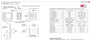
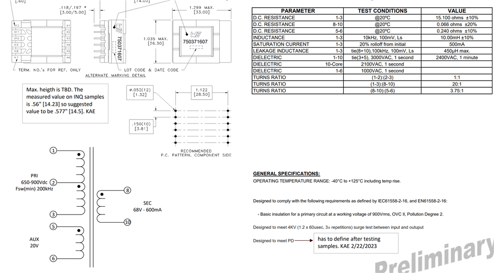
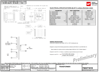
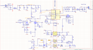
We have followed your EVM schematics and made a test board which does not start. The custom transformer is not made yet so we are using this off the shelf part just for trying out, pinout is different so we used short wires to connect correspondingly (attached datasheet).

Our PSU currently only provides 120V max so thats what we are testing at right now but i know this design should start at 100V, right? It draws 0mA. I have placed 1k load at 15V output node.

How can we troubleshoot this? What nodes should we measure?

P.S. We know that AUX is misconnected, that we have considered when mounting the transformer and mounted it correctly.
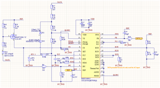
  • I have made a mistake by using IPD80R600P7ATMA1 as Q2 which is supposed to be a depletion mode mosfet. I will place the original Q2 CPC3982TTR tomorrow and update this thread with my findings.

  • Hello Valentinas, 

    I'm glad that you found that Q2 error before spending a lot of time on debugging.  
    However, there are other reasons why your board may not start up even after Q2 is corrected.

    Your substitute transformer (WE 7508112414) has greatly different properties than what the controller is programmed for (which appears to be the same as our EVM).
    Firstly, the substitute magnetizing inductance (460uH) is almost 3x that of the EVM transformer. 
    This means that to avoid being detected as a "shorted-CS fault" (see page 54 of datasheet), the input voltage must be 3x has high to start as for the EVM.

    Secondly, the substitute Aux-to-Sec turns ratio is much lower than 1 (actually, only up to 0.643 if both Aux windings are used) which will not provide high enough AUX voltage to keep VDD above the UVLO level after switching starts.  So even if the board got past all potential faults at start of switching, it would only be able to switch for more than a few milliseconds before running out of VDD.   

    Although there may be more issues that could interfere with successful start-up (not even addressing steady-state performance), these first two items indicate that a careful evaluation of the parameters of a proposed substitution must be made to assess the possible effects of each deviation from a designed parameter.  Small deviations may work, with some constraints; large deviations probably won't work. 

    On the other hand, if the transformer shown in your schematic (WE 750371607?) is the actual part that you want to use true, then it also has the wrong Nas ratio.  The text says Nsa = 3.75:1, which means Vaux will only be ~4V when Vout = 15V.  That will not sustain VDD either. 

    If you provide VDD with an external 15-V source (through a diode), the substitute xfmr still won't match the rest of the power stage and control values, and I can't predict what problem will arise first.  Switching frequency could be much lower than expected which could cause problems in ABM.  
    RDM and RTZ are calculated for the real xfmr, and their operations will be grossly off with the proposed substitute.  OVP will be way off, etc. 

    Until your designed transformer arrives (and hopefully it is different than either of the two discussed above), I suggest to look for a substitute with parameters that match the design much more closely.  Make an assessment of the impact of the deviations from design point, and decide if you can "live with" those impacts temporarily.  After finding a suitable candidate, plug in the substitute's actual parameters into the equations for RDM, RTZ, Rvs1 & Rvs2, Rcs, etc. and adjust the board values (temporarily) to allow better operation until the real xfmr comes in.  Then restore the correct values.

    After a little more perusal, I also noticed that your shunt regulator U3 is listed as TLV431 which has 1/2 the reference voltage as the EVM's ATL431. 
    Unless the TLV431 symbol is merely a pcb foot-print placeholder, you won't get 15V out of your board. 

    I also noticed a disabling-switch Q4 on the REF net.  This Q4 part number corresponds to a depletion-mode FET, so it will always be on, regardless of drive from the opto U5.  I suspect Q4 should be a small-signal enhancement FET.   

    Regards,
    Ulrich

  • Dear Ulrich,

    Thank you so much for your help.

    Our output voltage will be 68V in the end design, i am glad you spotted the winding ratio being different so of course i will need to increase from 15V to much higher for this test board. I will also account for TLV having a different reference voltage.

    Since the inductance in alternative transformer is higher, i calculated that i will need Rcs of around 0.9R to start up at 50V. Will do the change and see how it goes.

    Below is the transformer design thats coming to us next week. Do you think there will be issues with using it as with the configuration provided in its datasheet? Of course converter components will have to be adjusted.

  • I double checked both TLVs and they both have 2.5V reference, even placed mine over the EVM and the EVM still outputs 15V.

    I have placed in the original depletion nmos at Q3. Removed Q4. Placed around 2R Rcs, set Vout at around 31V. Tried input voltage up to 120V, output does not become active. Gate is always 0V, Vcs is 0V.

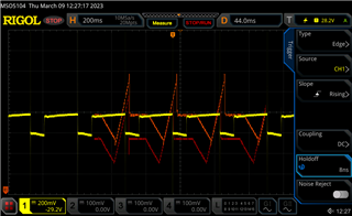
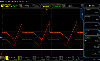
    Vin during below measurements is around 32V.
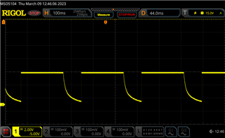
    Yellow is Q3 drain. 200mV/div. 200ms/div.
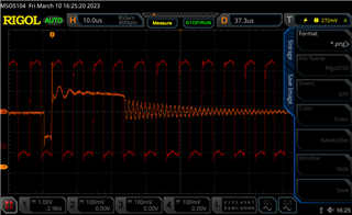
    Orange is Q3 source. Red is Q3 gate. 2V/div. 100ms/div.
     

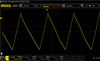
    Below yellow is Vref. 2V/div. 100ms/div.                      VDD:

    Do the graphs make sense?

    I am looking into equations for RDM, RTZ, Rvs1 & Rvs2, are they essential right away or can i use EVM values for now? I just want to get started somewhere before i start changing too many values.

    What else can i measure to debug this?

    EDIT: I can see that my RUN and FLT pins are low, trying to find out why.

  • How come i calculate 190k for EVM Rrdm value while your EVM uses 93k?

  • Hello Valentinas, 

    Thank you for the additional information.  It is going to take me a little while to analyze it all and provide some meaningful guidance.

    But let me address your last question first.  I agree with your RDM calculation and you do have a good question.  At this moment, I don't know why the EVM uses ~1/2 the value that the calculation recommends.   Following up on some development history, the UCC28781EVM-053 design was mostly copied from a previous PMP22322 reference design which in turn was modified from an earlier PMP21552 design.  I think several changes were made along the way involving Lm, Npa, and Rvs1&2, but RDM was apparently not updated as these parameters changed.  Interestingly, the EVM still works so the PWMH control (which drives the SR for ZVS) is able to compensate for the under-value of RDM.  I'll have to investigate this situation some time when I get a chance.  

    In your prior post, the REF and VDD waveforms make sense, but the two above them with 3 traces do not make sense to me.  They look like composites of three different sweeps pasted on top of each other.  The red and orange are vaguely similar but not coincident.  Still, some things may be gleaned from this. 
    You say you placed a depletion-FET at Q3, but Q3 is the SR Fet.  I assume you meant Q2.   
    In your EDIT, you report that RUN and FLT are low.  If they are always low and never pulse high even briefly, then there is a fault that prevents switching from starting.  The RED trace, which is Q2 gate which is HVG seems to drop from the peak of ~17V to 11V almost instantly may be the culprit.  

    During the initial part of start-up, P13 tracks VDD closely.  At the turn-on threshold (near 17V), P13 is shifted to become a regulated 13V source and its voltage is normally bled down to 13V with a small current.  If there is an open on P13, it will drop to <14V very fast. 
    Table 3 (DS page 53) indicates an open-P13 fault that prevents switching and cycles VDD through UVLO, which is what appears to be happening. 
    Please check the connection of P13 at the controller and to the FET. 

    As I mentioned, I'll need some time to digest the transformer information. 

    Regards,
    Ulrich

  • Hi Ulrich,

    I did indeed talked about Q2 depletion-FET.

    I have measured P13 on EVM, it looks exactly the same before Vin reaches 100V. Also measured the P13 fall time with Vin 30V, i see the same fall time on EVM and my board, which is 1ms and not faster than 10us so fault should not trigger.

    On EVM, at Vin 32V, the RUN signal is low. How come at 100V the EVM knows that its time to start? I do not see any pins whose value varies with the Vin, they all seem to be fixed or zig-zagging.. Does it internally know? I am very confused on how to troubleshoot this.

    EVM gate at Vin 32V is always low, how does it know that the Vin is 100V? How does it know when to start?

    EVM FLT pin measurements: orange shoot happens every 1.6s or so, it is at Vin 32V, 200mV/div, red is at Vin 100V, 1V/div. 

  • Hello Valentinas, 

    Okay, it's good to know that the fall time of P13 is much slower than 10us, so you're right, that will not trigger a fault. 

    But something is triggering a fault, so we'll have to look further to find it. 
    In the datasheet, Table 7-3 and Table 7-4 are lists of faults that result in shutdowns under various conditions.
    You report seeing no gate drive, so that narrows down the possible faults to those that can occur before any switching happens.  

    But first, let's verify two things: a) there is absolutely no gate drive pulse (no PWML) when VDD reaches the 17-V turn-on threshold, and b) there is no RUN signal when VDD reaches 17V.   You have to trigger on these signals with sweep speed of 2us/div to see them.  At 100ms/div, they may not be visible and you may think they are not there.  If they ARE there, you have to look at a different set of possible faults. 

    Assuming RUN and PWML are not present, then from Table 7-3 it could only possibly be OTP fault on the FLT pin.  If FLT is held low before start-up it will prevent switching and simply stay in the UVLO reset cycle (which is what you are seeing on VDD). 
    Other fault possibilities are in Table 7-4, which are all those where "Delay to Action" = "none".   

    From Table 7-4, we have ruled out "P13 pin open".  For the remainder, please check:
    1.  XCD pins are connected to AGND;
    2.  RDM and RTZ resistor values on the board match the values on the schematic, and are connected to the controller pins.

    In Table 7-4, there is also the "CS pin short" fault, but this fault requires a single pulse on PWML (and RUN also goes high for this pulse).
    This fault is the reason that the EVM starts at ~100V.  As discussed below the Table 7-4, in Section 7.4.13.1, Vcs must reach 0.2V within 2us on the first pulse or a fault is assumed.  Using V/L = di/dt, with the EVM inductance of 160uH and Rcs = 0.1662R, Vbulk must be > 160uH*(0.2V/0.1662R)/2us = 96.3V to meet the <2us criterion to avoid shutdown from "CS pin short" fault.    

    For your 460uH substitute transformer, it will take 3x higher Vin to start-up, unless you also increase Rcs value to compensate.  
    I suspect that this is why your board will not start up.  But you had said that you see no gate-drive or RUN pulses, so that's why I recommend above that you verify that first.  You may be missing them, because the "CS pin short" fault also keeps the UVLO cycling for 1.5 seconds before allowing another attempt at switching.  At slow sweep, it is easy to miss a single 2us pulse repeating only every 1.5s.     

    Regards,
    Ulrich

  • Hello Ulrich,

    I have confirmed that XCD is grounded, RDM and RTZ have correct values and seem to be connected to pins.
    CS pin was shorted to GND, i fixed it so now i can see gate 


    On my test board i have placed Rcs 1Ohm so it should turn on at around 50V, seems to try to turn on at 55V.

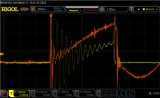
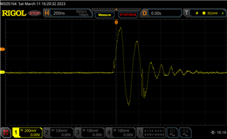
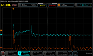
    Below is EVM QLSRC voltage. Orange is EVM 50mV/div, Vin 95V. Yellow is my test board, 100mV/div, Vin 50V, right before it turns on.


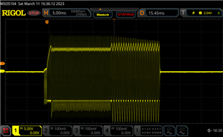
    My test board after QLSRC > 200mV (tries to start switching). This happens around every 15us and lasts for 30ms.


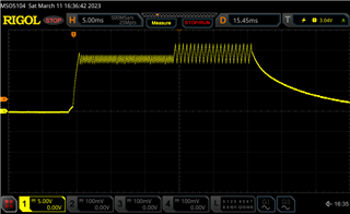
    Gate voltage. Vin 60V. Something happens after 15ms and after 30ms it stops switching.


    Below are output voltages. They happen every 1.5s, Transformer makes a sound but the higher Vin, the flatter the waveform, the lower the sound and my PSU shows lower current (during 30ms switches).

    Aux voltage straight at transformer output pin:                    Sec voltage:


    Why does it happen every 30ms? Why does my gate voltage start to go down after 15ms? What else can i measure to debug this?

  • Hello Valentinas, 

    I'm glad that you finally got your board to switch.  Now to try to keep it switching.

    In your first waveform there is tremendous ringing on the QLSRC signal (basically the current sense signal).    
    This indicates a large amount of interwinding capacitance in the primary winding. 
    This can be confirmed with a current probe monitoring the primary winding current.  This is a good signal to have anyway, so I recommend to take steps to insert such a probe.  The best place is at the primary winding pin connecting to the bulk voltage rail. 

    The second waveform appears to be the first (or one of the first few) narrow pulse(s) at the start of switching.  It appears to be showing the LC ringing of the first waveform photo, only limited by the on-time.  If that is not what it is, I'll need more context around this signal to figure it out.  Like the having PWML signal for instance.  

    Phot 3 shows PWML (gate voltage) at normal 13V for ~15ms, then it falls off to ~10.5V and stops.  This indicates that the VDD capacitance is holding VVDD up above 13V for 15ms, then VDD falls below 13V and P13 falls with it and so does the amplitude of PWML.  When VDD reaches 10.6V, the controller shuts off and begins a UVLO cycle to restart.  VDD can't stay above UVLO if the secondary output voltage does not or cannot rise high enough to reflect >11V on the Aux winding.  

    The last two photos are very strange to me.  However, you mention that they recur every 1.5s which tells me that the shutdown is due to any one of several possible faults listed in the fault tables in the UCC28781 datasheet.  Table 7-3 and 7-4 (pages 45 and 53, respectively) indicate all the faults that the device can detect and how it responds to them.  The ones with "tFDR restart" in the ACTION column are the ones to consider, since the response to these faults incur a 1.5s delay between restarts.   It is a process of elimination, to throw out those obviously not happening and narrow down those that are most likely to be happening. 

    All that current sense ringing may be triggering the CS-Open fault in Table 7-4. Even though it physically may not be open, the condition that the IC is detecting may be matching the symptom for the fault.  Still, it may one of the other tFDR faults. 

    The last photo (of Sec voltage) shows two different levels of zig-zagging on Vout.  (I assume it is Vout.)  I don't know why there are two levels, but this symptom resembles an unstable on/off control from saturating feedback currents.  I suggest to probe the collector of the feedback optocoupler to see if its voltage is going up and down at the zig-zag frequency.  If so, then the shunt regulator (TL431?) may not be getting sufficient bias current.  

    Regards,
    Ulrich

  • Hello Ulrich,

    The duration before it starts to shut off did increase after i added VDD capacitance, but that does not help with the main issue - low secondary voltage.

    Optocoupler collector voltage looks stable, no swinging during Vout swinging.

    I am trying a different off the shelf transformer and QLSRC does not ring as much, not sure if its because how i mounted it since the footprint is different or if its just "better".

    With the first transformer (https://www.we-online.com/components/products/datasheet/7508112514.pdf) i had around 13V sec and 8V aux output. 

    Now with the second transformer (https://www.we-online.com/components/products/datasheet/7508112330.pdf) i am seeing around 6.5V sec and 8V aux. 

    So, the Nsa makes sense. What does not make sense is why am i getting such low Sec output voltage even if i tried adjusting R31, R25, R26, R9. Only R9 seems to make a small difference but barely any. I have R31 = 10k and R25 = 150k, so i would expect few times higher Vout than what i am seeing. Vout does not change with different Vin, only the ripple and audible sound seems to be affected.

    Kindly,

    Valentinas

  • Hello Valentinas, 

    I don't know why you are getting only 6.5V output, but apparently you are hitting some unknown limit. 
    Simply changing transformers and a few resistors is not enough to expect a working design.  Your project really should be designed from the ground up, not modified extensively from a previous design.

    R31 = 10k and R25 = 150k on a shunt regulator with 2.5V reference should regulate to 40V output... when everything else is also working properly. 
    But the shunt regulator needs proper bias current to regulate, too.  Previously, you stated "I double checked both TLVs and they both have 2.5V reference...".
    A TLV431 has a 1.24V reference.  A regulator with 2.5V reference is not a "TLV" part.  The schematic diagram shows a TLV431 symbol, but if the reference is 2.5V (or 2.495V for certain parts) then it is not a TLV.   That had confused me earlier.

    Given a 2.5V reference, 10K and 150K corresponds to a 40V output setting.  I was staring at the schematic and happened to notice that the SR-FET driver secondary-side VDD is connected to Vout.  That is fine for a low voltage output, but the UCC5304 has a maximum rating of 20V on VDD.  
    So it is possible that the first time you applied power, Vout may have been climbing up toward 40V, but once past 20V the driver may have blown up and now maybe preventing Vout from rising past 6.8V.  
    I'm sorry that I didn't see that before, but the schematic also says 15V for the output and I learned of the intended 68V only later. 
    Of course, now we know that the VDD will need a regulator of some sort, to limit VDD.  Ideally to about 10V so Vgs is not excessive.  
    Ultimately, you can consider another secondary winding for this purpose, but that can be worried about later. 

    Back to the second transformer:  The turns ratio is better for AUX when Vout is 15~20V.  But if Vout will go to 40 or 68V, then the AUX winding voltage will be too high for the controller VDD.  Every time you make a change, it affects several other functions.  The higher Lm of 800uH (and higher leakage L) will also have significant ramifications on conversion behavior.  The Nps ratio would reflect 333V to the primary when Vout = 40V.  That could blow up the primary clamp TVS, D9, at 150V rating.  

    This shotgun approach to development is blowing holes everywhere but not really hitting many targets. 
    Instead of trying to repurpose the EVM design, I recommend to start your design from scratch so that all the component values are determined based on actual target parameters.  I do concede that TI does not currently have a dedicated design calculator for the UCC28781 yet.  However, the UCC28782 design calc tool can be used to determine the power stage parameters.  The portions involving the active clamp and high-side FET can have dummy values entered to avoid problems generating component values for the ZVS design.  Hopefully, using this tool will give you the full design required from the ground up, rather than working backward from EVM values and hoping not to overlook something.    

    Regards,
    Ulrich

  • Hello Ulrich,

    Since the board was hand mounted, i decided to build one more. At first i had other issues but those turned out to be soldering errors. Eventually it started to progress, now i am seeing output for 160ms, then it goes off.

    Btw regarding TLV being 1.24V, you are correct, but i actually have TL431, which does have 2.5V ref. Its a graphical error in the schematics.

    Regarding gate being able to handle only 20V. i did realize that and patched in a 10V zener + 100R to limit current, so my gate driver is protected. Forgot to tell you about this.

    So, as i mentioned, im now seeing a nice output for 160ms, then it goes low. Repeats after 1.5s (restart happens).

    21.5V AUX

    33V Vout

    3V Vvs (Rvs2 i have 3.3k instead of 6 98k as in EVM).

    It cannot be Vovp because it goes up to just 3V, no overshoot. So, the next possible scenario is Vopp. What do i measure and calculate for this? Currently i have EVM value 402R for Ropp. 

    What i find strange is that Vout is not easy to adjust, i am not able to reduce it slightly, it makes no difference if i change R25 and R31 but if i make a big enough jump, it just drops Vout to like 25V which is then too low for Vaux to take over VDD. I probably need to adjust other resistors, but i did not have the time yet to read through. Do you have a hint? Too large R25 R31 values maybe?

    Thanks for the help,

    Valentinas

  • Hello Valentinas, 

    That is good news about your new board and protecting your SR gate driver. 

    This is not an OVP problem.  The 160ms time limit is a direct result of over power protection (OPP).  Nothing else has this specific timing.
    OPP means that the peak primary current is exceeding the OPP threshold and this is allowed for up to but not greater than 160ms continuous duration.   

    Design for normal rated power would result in steady-state primary current peaks operating below one of the dotted OPP limit curves of Figure 7-43.  
    The limit curve being enforced (either blue dotted curve or brown dotted curve) depends on whether the voltage level sensed at VS input during the demag time is < 2.4V (blue) or > 2.5V (brown).  Current peaks may exceed the dotted lines but are strictly limited by the solid lines for a maximum of 160ms. 

    Ironically, Ropp has little to do with setting the OPP level.  That is designed by choice of Rcs, together with other factors. 
    Ropp is used to compensate for turn-off delays and mainly adjusts the OPP level at high input voltage to accommodate for such delays. 
    Right now, Ropp is of little concern.  

    Anyway, this kind of situation (shutdown after 160ms) usually happens when there is an overload (not necessarily short-circuit) on the output.  
    Alternative causes can be:
    a) actual power limit is lower than intended power limit (usually due to a design mistake or assembly error).
    b) feedback loop open or stuck at a fixed level (also usually due to a design mistake or assembly error).

    The fact that your Vout is not easy to adjust strongly suggests that your feedback loop is "not working".
    That can happen from various causes, but most likely it is because your TL431 is not biased correctly by R32. 
    The UCC28781EVM-053 uses 5.6K which is appropriate for an ATL431 regulator, but this value is too high for TL431.  
    Please set R32 = 560R, to deliver the required Ika for TL431. 

    Also, the TL431 has an Abs Max limit of 37V for Vka, so going to 40V output can damage it.
    Since we're just trying to get steady-state operation at this point, I suggest to target Vout = ~30V by setting R25 = 150K, R31 = 13.7K.   
    Using 7508112514 and full Aux winding from pin 4 to 6, that should provide ~19V to the primary VDD.  

    Because the actual power capability of your board is unclear, I suggest to apply a light load to your output.
    This converter will always start into maximum current while it is charging up the output caps, but should be able to finish charging well before the 160ms time limit is up and subside into a light-load regulating mode.  If it doesn't then it has other problems and we'll have to debug and eliminate them.
    I also suggest to short out L6 and L5, to keep them from adding issues.  The TL431 should be regulating VOUT+ to OUT-, or at least VOUT_F to GND; not VOUT node.

    I hope this gets you to a steady-state operation.

    Regards,
    Ulrich 

  • Hi Ulrich,

    You were right about the feedback loop. I made a mistake by placing the gate 10V zener on the common net as for the TL431 so its reference was being fed 10V constantly. I fixed this patching error and now im getting the programmed voltage. It was causing the over-power protection. 

    At higher Vin it goes into OPP mode but if i adjust the Rcs, it allows me to increase the Vin. 

    I wont receive my 900V supply until a few weeks from now but i will get something close to it in the meantime. 

    Now im thinking - i will need to a add over 30V of series zeners to drop the excess of 68V from TL431.

    I want to calculate my OPP setting but the formula asks for td(cst) input and i dont know what its equal to. Is it a standard or varying value?

    Have you made any calculations will it work at 30W with my 10mH transformer at 650-900Vin and 68Vout?

    Thanks for your patience!

    Valentinas 

  • Hi Valentinas, 

    It's good to see some real progress. 

    I have not made any calculations yet, but your question makes me wonder what the actual design targets are. 
    Previously, we were shooting for 15V, then 40V, now 68V.  The documents above refer to 600mA output, now Pout = 30W which means Iout = 440mA.
    Startup was 100V trying for 50V, now input appears to be 650-900Vdc.  

    Before doing many more calculations, I'd like a list of the actual design targets for input and output, including special cases and limitations and desired start-up voltage. 

    Here are some issues that I find, with the information available so far:
    1.  800-V rating of CPC3982 will not do well with 900V input plus reflected voltage on primary. 
    2.  Transformer design 750371607 (10mH) has Nps ratio of 20:1, so reflected voltage = 1360V at Vout = 68V.   That ratio is good for a low voltage on the SR FET Q3, but bad for the stress on the primary FET Q1.   Also dielectric rating from xfmr pin 1 to pin 6 (1000VAC) is inadequate for the peak voltage expected  between these windings.  
    3.  D9 will not survive with 1360V reflected back.  Neither will D2, but D2 is not necessary.  
    4.  I noticed that the AUX winding polarity in the schematic diagram is backwards.  Pin 5 should go to HV_GND.

    For the Rcs equation (17), td(cst) is described in the paragraph just below the equation as a summation of a few different delays.  Of these, td(cs) is specified in the Electrical Characteristics table (page 8), you don't have a low-side driver, and CS filter and Coss delays must be estimated.   It is too soon to be too accurate about this calculation.  Since a SiC FET has fairly low Coss, an educated guess would be to use td(cst) = 75ns total.  

    I wonder if the transformer design needs to be rethought, which will involve making trade-offs with the semiconductor ratings.  
    Please note: I am going to be out-of-office this coming Monday.  If someone else covers this thread, they may need a lot of time to come up to speed on the issues. 

    Regards,
    Ulrich

  • Hi Ulrich,

    Sorry for the confusion.

    The final design will have:

    650-900Vin

    68Vout/600mA

    The reason i have been changing things one by one is to understand how everything works and the dependencies. I want to slowly get to the final design.

    I understand about the possible overshoot issues, but that can be solved.

    Right now we are stressing about locking the transformer design so it can go for a small volume production because we will need that ready this summer.

    Now I have connected the 10mH transformer and its not doing what I expect it to. I also have a 4mH version so i might try that.

    Vin 165V. Yellow Vout. Pink Vaux. Blue Vrcs (Rcs = 2.2R). Keeps doing that every 1.5s.

    I am still early into this investigation but Vout looks very low. I am really confused about this. Any tips here?

    Thanks,

    Valentinas

  • Hi Valentinas, 

    We have reviewed this issue before.  This is a recurring start-up fault because your Vin is too low to overcome the "CS-short" fault time limit of 2us. 
    Vcst(sm1) threshold = 0.2V/2.2R = 0.909Apk.  With Lm = 10mH, tON to reach 91mA = 0.01*0.091/165 = 5.5us. 
    You'll need Vin > 455V to overcome this fault.  

    For lower Vin start, you can overcome that using 6.8R+ at Rcs, but you won't get full power.  It would seem to be worth testing though, to get past this hurdle and see what's next.  However...

    Your statement about "...possible overshoot issues..." concerns me that what I'm trying to convey is not being understood.
    I'm not talking about mere overshoots, I'm warning that your primary circuit will experience exceptionally high sustained voltages for a few cycles before it blows up.  These are not overshoots or transients that can be clamped or snubbed out.  
    Most of this stress comes from the 20:1 Pri:Sec turns ratio.
    I think the transformer definitely needs a redesign. 

    Your comment about trying a 4mH option also raises concern.  You've been making changes one-by-one to understand dependencies.  I've been trying to show that this design has many interdependencies, where changing one parameter often requires changing more than one other parameters to accommodate the effects of the first change.  This is an extremely slow way to get to the final design, and in my opinion not likely to improve understanding of what's going on.  Or, of what should go on.  We haven't even gotten to what I anticipate to be the real problems to be solved once the design is mostly settled, such as how well the ZVS works, actual vs. expected efficiency, and possible self-interference from di/dt's and dv/dt's, for example.   

    Making calculations for the final design up front will tell you what practicable tradeoffs will have to be made in the component selection, since primary FET ratings and availability are limited.  And it will avoid acquiring the false notion that something easily done at low voltages will be just as easy to accomplish at 900V.   

    Regards,
    Ulrich

  • Hello Ulrich,

    I made the test board work with 460uH and 800uH off the shelf transformers, but i am having troubles with 4mH, 10mH. 

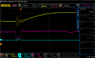
    In the picture above you can see the blue line (Vrcs) is high enough for the controller to start but the signal is not stable.

    In the picture below the blue line is a 460uH transformer which i have no problems with, but the 4mH transformer (Vrcs red, 500mV/div) looks completely wrong.
    After lots of Rcs adjustment and voltage increase i can make it try to turn on but immediately it starts to produce huge spikes >1.2V which is basically the red graph, which makes it trigger Vocp. I am already at 0.44R @320V so if i reduce Rcs to 0.4R then it wont start at all @320V. If i just increase the voltage to around 335V then it starts and immediately triggers overcurrent protection.

    I tried various Ccs capacitances (300p,1n,1.5n, 2.2n, 3.3n, 4,7n, 6.8n, 10n). At 2.2n it doesnt even reach minimum Vcs, at 1.5n tries to start but as soon as it starts to switch the Vcs goes so 3V, due to inductances.

    It looks like the transformer with high inductance (+high leakage and interwinding capacitance) cannot be used with this IC or it will keep triggering overcurrent.

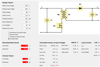
    Below is the Lm calculation. What happens if the transformer has 1mH under same voltage/current conditions? Will it just try to increase the frequency? So basically in this calculator we can enter say 900kHz which gives us a calculated 1mH recommendation and everything will work just fine?
     

    I suppose EMI is much worse at higher frequencies? Or maybe its easier to solve because smaller EMI filters are needed?

    Thank you!

    Valentinas

  • Hi Valentinas, 

    To address your points and comments: 

    1. "In the picture above you can see the blue line (Vrcs) is high enough for the controller to start but the signal is not stable."
    I disagree with your assessment of the blue trace.  On a 500mv/div scale, the highest point of ringing in the middle of the on-time does not rise to or above the 200mV threshold to terminate the first pulse.  At the end of the pulse, the ringing is only about 100mV and the 2us timeout generates a "CS-open" fault.    

    2.  "In the picture below the blue line is a 460uH transformer..."  
    Here, the blue trace still has ringing, but steadily climbs toward 200mV and apparently just makes it within the 2us time limit to avoid the fault. 
    The red trace shows that Vcs is already above the 200mV threshold at the moment that the leading-edge blanking time (tLEBCS) expires (200ns), so the on-time is cut off.  The recurring pulse means that start-up is being attempted, but there is insufficient energy in the magnetizing inductance to charge the output and support VDD.  The high current within the 200ns tLEBCS window is due to discharge of the high winding capacitance of the 4mH transformer.  

    3.  "It looks like the transformer with high inductance (+high leakage and interwinding capacitance) cannot be used with this IC or it will keep triggering overcurrent."  High inductance is not an overcurrent issue (although it can pose other issues, which may be mitigated), but it is the discharge of high interwinding capacitance that keeps triggering overcurrent. 

    4.  "I tried various Ccs capacitances (300p,1n,1.5n, 2.2n, 3.3n, 4,7n, 6.8n, 10n)."  This is again a shot-gun approach without understanding the ramifications of such high capacitance at CS.  You are attempting to filter out the leading spike, but the R-C time constant formed from Ropp*Ccs also results in a time delay of the voltage slope generated from the primary di/dt though Rcs.  Higher an higher Ccs means longer and longer turn off delay, so your cycle-by-cycle peak current will get higher and higher.  Much higher than the peak level that the maximum Vcst would normally allow.  
    The real solution is to wind the transformer in a way that minimizes capacitance.  
    If that fails to solve the problem, then the leading edge blanking time must be extended externally with a transistor circuit driven capacitively by the PWML signal.  Such a circuit is often used with flyback and forward-mode controllers without LEB. 

    5.  "Below is the Lm calculation." 
    I don't understand your conclusion.  The two top red boxes of the calculator recommend 6.23:1 ratio and 4.52mH of inductance.  The two bottom red boxes show choices of 1.33:1 and 14uH.  These choices are so far from what is recommended that the calculated results are practically meaningless.  
    6.56Mhz frequency with 20ns on-times?  
    I recommend to choose values which are close to or equal to the recommended values, and then assess the results.  

    Regards,
    Ulrich 

  • Hello Ulrich,

    An off the shelf transformer with lower inductance seems to work well. We will use it for the low voltage isolated conversion.

    Now i need to make this work with my 4mH transformer for HV isolated conversion.

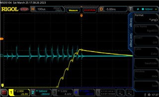
    Below blue is Vcs and yellow is Vout. I need around 40V there for Vaux to get enough voltage to keep it alive.

    If i adjust TL431 resistors, its pin1 changes but Vout does not.

    If i reduce optocoupler resistors, TL431 pin1 goes up but Vout does not change. Currently i have 510R at R32. Tried various R26 values - how is it calculated exactly? On my LV converter i had to reduce is to 11k to make it work.

    I am using 0.5Rcs and it starts to "try to switch" at around 530V. At higher Rcs it did not even reach 26.8V, but it looked like it was OPP triggering.

    This repeats every 1.5s.

    Vcs does not go above 1.2V, so why does Vout stop increasing?

    Vvs goes to 2V by the time Vout reaches 26.8V

    FLT is at 2.4V.

    Any ideas?

    I will order the version without OPP and see if this solves the problem.

    Kindly,

    Valentinas

  • Hello Valentinas, 

    Vout stops rising because the switching stops. 
    An OPP fault is characterized having peak Vcs pulses (not including leading-edge spikes) that continuously exceed the Vcst(opp) level (see Figure 7-43 in datasheet) for a duration that exceeds160ms.  
    The screen shot shows some pulses with diminishing peaks that last about 0.5ms.  This does not constitute an OPP fault. 
    Some other fault which involves a 1.5s shutdown time must be causing it.  

    Please review the Fault Protection Tables 7-3 and 7-4 to identify the possible faults which match the timings and investigate for symptoms of each possibility to eliminate those faults that don't match the symptoms listed.
    Note: the IC acts on signals that it sees at its input pins, not on what is out in the power stage.
    If the signal levels at the pins point to an OVP shutdown (for example) even though Vout is no where near OVP level, then look for errors in VS divider resistances and/or turns ratio.  

    Never assume that the pcb assembly is exactly equal to the schematic diagram.  
    Many times, the schematic is fine but errors were made in constructing the board. 

    That said, the behavior in your latest screen shot is curious.  
    Normally during start-up, peak current goes high and stays high until Vout approaches its target level.  
    This is because the TL431 normally stays off (Vka roughly tracks Vout going up) until the feedback reaches the REF level. 

    In this case the current peaks are diminishing, which means Vcst is reducing as Vout rises, which implies that current is increasing in the opto-coupler photodiode.  Higher diode current means higher collector current which is higher FB current which reduces Vcst.  
    So regardless of what is shutting off the switching, the reduction if Ipeak is a symptom of another problem which indicates that something in the TL431 block is not working right.  

    As I mentioned before, the TL431 Vka is limited to < 37V, so a clamp is needed on the voltage at R26 to avoid damaging the TL431.  
    You had mentioned that you made modifications in this area to limit VDD stress on the isolator. 
    I have not seen an updated schematic diagram since your first post, so there may be some error in the modification or on the pcb.  

    Regards,
    Ulrich

  • Hello Valentinas, 

    I've seen no correspondence on this E2E thread in about 2 weeks.  
    If you have solved the problem, then I'd like to close this thread.  

    Regards,

    Ulrich

  • Hello Ulrich,

    The thread can be closed, although i have not suceeded in making it work with a 4mH transformer. It did work with some off the shelf 800uH, which indicates that most likely the parasitics was the cause.

    We did not have the time to troubleshoot it further so we went with UCC28C56H which has worked with the 4mH transformer.

    UCC28781 works with our low voltage design so we will still use this IC there.

    Thank you for now.

    Valentinas