This thread has been locked.

If you have a related question, please click the "Ask a related question" button in the top right corner. The newly created question will be automatically linked to this question.

TPS62913-IBB-EVM: Question about the EVM User Guide

Genius 4220 points
Part Number: TPS62913-IBB-EVM
Other Parts Discussed in Thread: TPS62913, TPS82130

Hi,

I'd like to know the following things about the VOUT ripple data of TPS62913-IBB-EVM.

About Figure 2-2. Output Voltage Ripple, Measured at J5 (After Ferrite Bead), when you captured the waveform, where was the FB line connected to after the ferrite beads or before? 

Regards,

Go

  • Hello, 

    The FB was connected at the first LC filter, not after the ferrite bead, as shown in the schematic (Figure 5-1) with R12 not populated.  If R5 is removed and placed at R12, then the FB will be connected after the ferrite bead.

  • Hi, Steve

    Thank you for your comment.

    I understand that the Figure 2-2 was captured under the default condition of TPS62913-IBB-EVM.

    I'd like to know the following things about TPS62913-IBB-EVM,

    1. About the input capacitors of TPS62913-IBB-EVM, according to the Figure 5-1. TPS62913-IBB-EVM Schematic, input caps are mounted between VIN and GND only.(C1 to C4)

    I suppose we should place some caps (like 10μF+0.022uF) between VIN and PGND as described in the APP Note below.
    (www.ti.com/.../snva856b.pdf)
    Is there any particular reason that some caps between VIN and PGND are not implemented on TPS62913-IBB-EVM?

    2. If I need to change output voltage to -1.6V, we should replace R5 values to 29.4kΩ, is it correct?

    3. If the FB is connected after the ferrite bead like you mentioned, do you think output ripple voltage and output spike (see in Figure 2-2 of EVM user's guide) will be improved?

    Regards,

    Go

  • Hello, 

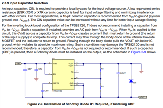
    For the TPS62913, it is not recommended to have a VIN-VOUT cap (sometimes called CIO or CBP) due to the stress it can cause on the VO pin.  If you find you need to use a CIO, it is recommended to use a diode across the output as shown in the following app note: https://www.ti.com/tool/TIDA-01457. The relevant section is shown below:

    I may include this in any updates I make to the TPS62913 IBB EVM User Guide, as this is not the first time this has come up.

    To change the output voltage to -1.6V, I would recommend that you leave the R5 value of 5.6k, and change R6 to also be 5.6k.

    For the FB location, moving the FB to the output of the ferrite bead filter will help with DC regulation over load conditions, but will not improve the high frequency spikes seen in Figure 2-2.  For the best stability, with a balance between output cap requirements and BOM count, I would recommend keeping the FB sense before the ferrite bead filter as configured on the EVM.

    Regards,

    Steve Schnier

  • Hi, Steve

    Thank you for your advice.

    I thought that TPS82130 IBB don't mount the CIO because the absolute max rating of VOUT is 0V.

    The ABS max rating of TPS62913 VO pin is -0.3V, but TPS62913 IBB still has the similar risk to get damage by CIO?

    Regards,

    Go

  • Hello, 

    Yes, the circuitry is similar for the VO pin and it has the same susceptibility.

    Regards,

    Steve Schnier

  • Hi, Steve

    Thank you for your comment.

    I suppose every device which use DCS control has same risk, right?

    And how about other DCDCs using different control, like DCAP-2 or DCAP-3?

    Do they also have same risk?

    Regards,

    Go

  • Hi Go,

    You are right. All Buck converters have same risk.

    Thanks,

    Nancy