This thread has been locked.

If you have a related question, please click the "Ask a related question" button in the top right corner. The newly created question will be automatically linked to this question.

UC3842: Instability Issue

Part Number: UC3842
Hi Experts,
I am posting this on behalf of the customer. Here it is below.
I'm designing a boost converter based on UC3842 as in the pdf file attached. It is showing instability when in full-load operation. Could you please help me to set up the right value for the compensation network? 
In a few words this is the problem:
the output voltage is regulated to 100V as I want.
The duty cycle in CCM should be 0,76 with an input voltage of 24V.
In steady state (Vout 100V and Iload 4A) on my scope I see 3 consecutive cycles with the maximum duty (limited by the PWM controller to 0,92) and 1 cycle at minimum duty (less than 0,1).
After that, the next pattern is the same, and so on.
The switching frequency is 160kHz.
I guess that the compensation network is wrong (R and C are connected to pins 1 and 2 of the UC3842). Probably both pole and zero are not in the right place in the Bode diagram.
Unfortunately on the datasheet, only a flyback calculation procedure is shown. I would like to have an example calculation related to a boost converter.
Thank you in advance.
Best regards,
Jonathan
Best regards,
Jonathan

  • Hi Jonathan,

    I see their expected duty cycle is 76% and this is current mode control.  Current mode control is known to have sub-harmonic oscillations (instability) above 50% duty cycle.  To remedy this they must add Slope Compensation.  Examine the datasheet for the recommended Slope Compensation circuitry.  Also, they should do a Google search for Current Mode Control and Slope Compensation.  There are numerous papers published on this topic.

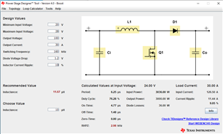
    For the compensation network: customer should download and become familiar with TI's (free) Power Stage Designer.  This tool will analyze the power stage AND enable them to use its Loop Calculator to examine the Bode plot of the system and set external compensation values.

    Here, I opened Power Stage Designer and selected "Boost Converter".  Then I entered target values based on their specifications and schematic (Vin, Vout, Iout, fsw, inductance, etc).

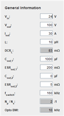
    Then I selected "Loop Calculator" and entered their typical Vin (24V) and estimated the (combined) ESR of their output capacitors, 200mohms.  They should enter the actual combined value for ESRout1 based on their capacitor part numbers / datasheets.  The ESR of the output capacitors is important because it sets a low frequency zero and could strongly effect the phase margin.


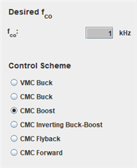
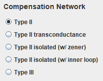
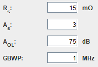
    Next, I selected "CMC Boost", "Type II" compensation, and entered values for Rsense (15 mohms based on their schematic), and RFBT (typically 38kohms based on their schematic), and current sense gain (As = 3.0 based on UC3842 datasheet).  Note that values in grey boxes are not part of their configuration.


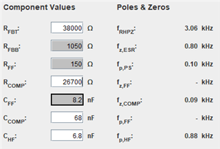
    Finally, I entered "real" values from the suggested values of Rcomp, Ccomp, and Chf: 26.7k, 68nF, 6.8nF  Note the calculated poles and zeros of the system.

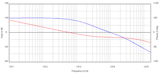
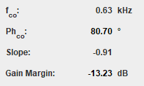
    At this point we can view the bode plot, 0 dB crossover frequency (630 Hz), phase margin (80 deg), and gain margin (13.2 dB).  This is a very stable system.  They should try these compensation values, but keep the duty cycle below 50% because they don't have slope compensation.

    Regards,

    Eric

  • Hi Eric

    Many thanks to your kindly support.

    Today I have ultimate the boost converter tests and finally it works very well.

    As you suggested, I used Power Stage Designer tool and I've got the right values of the compensation network.

    Regards

    Tiziano

  • Hi,

    Very good.

    I will continue to support in case needed.