This thread has been locked.

If you have a related question, please click the "Ask a related question" button in the top right corner. The newly created question will be automatically linked to this question.

LM5122: Programmable current limit in LM5122

Part Number: LM5122
Other Parts Discussed in Thread: LM5170, LM324, TPS63000, LM5176, LMP8646, UC3843

Hi,

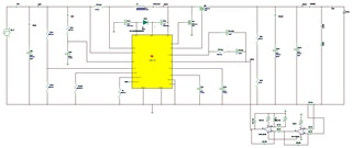
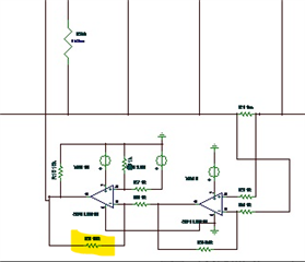
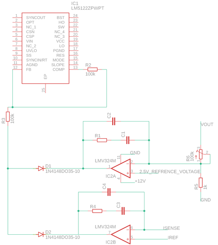
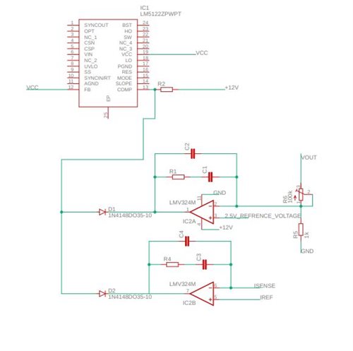
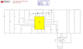
I am planning to use LM5122 multiphase boost converter for my application .  . following are my some queries.

1. Can we use multiple LM5122 to provide higher current output

2. Can you suggest some way to implement programmable current settings i.e by sending some signal from can we limit output current of the boost converter. The product on which i am working requires current settings from 1A to 30A. 

Regards

Mudit

  • Hello, 

    Thanks for reaching out. Yes, the LM5122 supports a multiphase configuration, at this link you can find some circuit examples: https://www.ti.com/reference-designs/index.html#search?keyword=LM5122 
    The PMP7969 (schematic here: https://www.ti.com/lit/df/snvr292/snvr292.pdf ) is for example a 4-phase design. 

    Let me try to clarify the second question: are you trying to set different values for the current limit of the device (which is the peak current of the inductor) or are you trying to have a constant current at the load independently of the input voltage value? We're looking forward hearing from you. 

    Kind regards,
    EM

  • Hello mudit mittal,

    Have a look at this device for the output current limit: LMP8646 data sheet, product information and support | TI.com

    Best regards,
    Brigitte

  • Hello,

    1.  PMP7969 (schematic here: https://www.ti.com/lit/df/snvr292/snvr292.pdf ) is for example a 4-phase design) can you please explain what is the fundamental of using external sync and how it works

    2. I want to operate boost converter in CC and CV mode . i.e if output current crosses more than a prescribed limit the boost converter will start working in CC mode , let the output voltage  vary and output current remain constant . 

    as par my understanding by changing the voltage at FB pin we can implement the above mentioned philosophy,

    To measure output voltage and current i have onboard microcontroller 

    Regards

    Mudit Mittal

  • Hello mudit mittal,

    1. LM5122 gives a 180 degree phase shifted signal to SYNCOUT for a dual phase system, if more phases are needed and other than 180 degree phase shift is needed (in this case 90 degree), external sync needs to be used like in the reference design you mention. In the datasheet there are as well other examples how to synchronize 4 LM5122.

    2. This is correct.

    Best regards,
    Brigitte

  • project i am planning to use LM5122 in CC mode .The current can be programmable by changing VS2 voltage.
    The circuit is not working as expected can you verify and let me know the issue' LM5122_CC_Mode_54VBATT_Programmable - autosave 23-04-17 15_20.TSC

  • HI Mudit,

    Can you share the input/output condition?

    It may be much easier for CC control with LM5170 Multiphase bidirectional current controller

    Best Regards,

    Feng Ji

  • input : 30V

    output : 1A

  • HI Mudit,

    What is the output voltage? Why do you use multiphase for 1A output?

    Best Regards,

    Feng Ji

  • Hi Feng Ji

    The actual output current goes to 62A. for simulation i use 1A as test cases. Also output voltages vary from 42V to 54V

    Regards

    Mudit

  • HI Mudit,

    You may consider LM5170.

    The benefit is as follows:

    • stronger gate driver for high power application
    • 2 phase interleaving in one controller and easy to extend to 4-phase
    • Accurate current sharing among phases.

    You can regulate the input current with voltage command.

    Best Regards,

    Feng Ji

  • Hi 

    I am following  PMP7969 (schematic here: https://www.ti.com/lit/df/snvr292/snvr292.pdf ) is for example a 4-phase design) , can you tell me what is the issue 

    going ahead with that since i already freeze my initial bom for boost converter

    Also pls tell me the issue with the circuit i shared 

    Regards

    Mudit Mittal

  • Hi mudit,

    You may go with the design now.

    You may need to adjust the compensation and you will also need voltage loop to avoid over voltage.

    Best Regards,

    Feng Ji

  • Hi Feng Ji

    Thanks . Can you share me any good document for designing cc cv loop using opamp 

    Regards

    Mudit Mittal

  • Hi Mudit,

    Generally you need two loops with ORing like below.

    https://e2e.ti.com/blogs_/b/powerhouse/posts/power-tips-how-to-control-multiple-loops-in-a-power-supply

    Best Regards,

    Feng Ji

  • Hi feng

    Thanks for the reply . 

    Following circuit is the part of LM5122 boost converter with following specifications:

    Vin : 30-40V
    Vout : adjustable upto 60
    Iout 12.5A at 60V
    switching freq : 200khz

    To implement CC-CV mode i have implemented following circuit

    1. The internal opamp is converterd into unity gain amplifier using R2 and R3

    Query : Is the logic is right

    2. The LM324 is used for opamp based type2 compensator :

    Query : Is the circuit is right,if not pls recommend the changes

    3.The external Vref is taken 2.5V

    4. to increase the current i am connecting 4 LM5122 in parallel .to synchronize i am providing external Fsync signal to
    pin no. 10 of all 4 Lm5122 ic leaving syncout unconnected.

    for switching frequency of 200khz shall i have to provide clock of 200khz or 400khz on the pin no . 10 of Lm5122.

    to generate the clock i am using microcontroller and CD4017 for frequency shifting. is the approach is right ?

    Regards

    Mudit

  • Hello Mudit,

    We will have a look at it and come back to you in a day or two.

    Best regards

    Harry

  • Hi Mudit,

    1. This is an inverting amplifier. You may need negative input for correct COMP voltage. You may connect FB to VCC to disable the internal OPAMP.

    2. Based on 1, connect D1 and D2 anode to COMP. Pullup resistor is required for COMP. You will loss soft start function with external OPAMP. 

    3.OK

    4.By connecting FB to VCC and OPT to GND, you should provide clock of 200kHz.

    Best Regards,

    Feng Ji

  • Hi Feng

    1 Can you explain more about statement "This is an inverting amplifier. You may need negative input for correct COMP voltage"

    2. Pull up resistor is for proper biasing of opamp ? pls comment

    Attached the new schematic

    Regards

    Mudit

  • Hi Mudit,

    1. COMP need to go above 1.2V for proper operation. You may find that the voltage input at R3 may be less than 0V.

    2. As both op amps can sink current only, you need a pullup resistor.

    Best Regards,

    Feng Ji

  • Dear Feng

    The circuit is not working as par the recommended changes . I simulated in Tina TI

    The boost operation is not happening. i am first trying to make CV  loops work 

    lm5122_adjustable_voltage_60V.rar

    Attached : simulation file

    Mudit Mittal

  • Hello, 

    Thank you for the feedback. Does your simulation run at all if you first just try to implement a simple boost without the opamp, but using instead the resistor divider to the FB pin (like for example the schematic of the EVM https://www.ti.com/lit/ds/symlink/lm5122.pdf )? 

    Kind regards,
    EM

  • Dear EM.

     simulation is working without opamp. can you pls check the simulation file which i shared

    Regards

    Mudit Mittal

  • Dear All,

    Can you pls suggest the solution

    Regards

    Mudit Mittal

  • Hello, 

    Thanks for your message. We are currently looking into this and will come back to you as soon as possible. Thank you for your patience. 

    Kind regards,

    EM

  • Dear EM

    we can control output voltage by  feeding current in fb pin of LM5122  following the application note "Dynamically Adjustable Output Using TPS63000".

    The  simulation model is working fine . attached for your verification. 

    Following are some doubts,

    1. Can we use same technique for CC CV control, if yes pls let me know the circuit

    2. I want to simulate battery in Tina Ti for cccv charging ,example the battery voltage variation with simulation time i.e initial battery will be cc mode and after some millisecond the battery voltage rise to  switch to cv mode

    lm5122_new_idea.TSC

    3.The above mentioned technique will work for multi phase desgin

    Regards

    Mudit Mittal

  • Dear EM

    Any solution to my issue

    Regards

    Mudit Mittal

  • Dear EM

    Request you to provide solution to my issue. 

    Regards

    Mudit Mittal

  • Hello Mudit,

    1. you can use the average output current sense function for operating the device in constant current. If the load commands more current than the IC is allowed to deliver based on the average current measurement through ISNS+/- it will operate in constant current. Then when the FB reaches the set output voltage, it will operate in CV as long as the load does request less current than set by the average current limit through ISNS+/-. So no additional circuitry needed.

    2. The average current function seems not to be implemented in the TINA model. So with this model, the CC function cannot be simulated. Best would possibly be to order an EVM and check it out in the lab.

    3. Yes, as this is standard function of the device, it will work for multiphase as well.

    Best regards,
    Brigitte

  • Dear Brigitte

    apologies for my limited understanding, following are my  queries

    1.The tina file which i shared ,is the circuit is correct or i have to do update the schematics

    2.I am planning to make a proto board depending on tina file which i shared for testing as tina ti  model is not giving me any result

    3. what is this average current function can you elaborated more and how this will be implemented

    4.why the tina ti model is not giving me result if i want to use external compensation in CV mode i.e using the external opamp with  FB pin pulled to VCC.  the model always have convergence error. the error is always ".dbd"

    5.Does the type 2 compenstaor parameter changes in CC CV mode . as i can't simulated CC CV mode  . how to calculate the compenstaor parameter for type 2 compensator for practical application

    6.i tried to simulate circuit in pspice for ti but the model is not converging

    7.as this is not the right forum for queries regarding the TINA ti software ,can you suggest me a proper document regarding TINA TI parameters definition

    Regards

    Mudit Mittal

  • Hello Mudit,

    Please excuse me, I answered too many questions in a row and had LM5176 is my head instead of LM5122. My apologies for the mix-up.

    1. I cannot find any current measurement in your TINA file, so how do you want to keep the output current constant without measuring the output current? LM5122 is regulating to a constant voltage, so you can use the device as is for the CV functionality, but you need to add a sense resistor in series to your load for keeping the current constant. Please have a look at LMP8646 for the circuit setup.

    4. Which TINA model are you talking about, the one that you can download from the TI website or the one you created?

    5. For CC operation, the current loop needs to be compensated. The voltage loop is not really doing a lot there.

    6. Which model is not converging? Did you download the one from the website? I think it is updated recently.

    7. Let me try to find something.

    Best regards,
    Brigitte

  • Dear Brigitte,

    The circuit model i generate form power designers tool . AS par the ongoing discussion with your fellow ti member to implement
    external compensation i pulled FB pin to VCC and comp pin is connected to external compensator with cc cv loop using opamp

    since the model is not converging in TINA o break the model in 2 parts CC and CV mode. the schematic and model i shared
    is CV mode with external compensation.

    When i trying to run the model it shows convergence error if i select calculate operating point in transient analysis it shows
    ".dbc" error and if i select zero initial value TINA ti models runs but boost operation does not works.

    Request you to look into the issue

     lm5122_adjustable_voltage_60V.TSC

    Regards

    Mudit Mittal

  • Hi Mudit,

    I am very sorry that the models show convergence issues.
    If I understand correctly, the convergence issues occur both in TINA and PSpice simulations, correct?
    As PSpice is more modern than TINA, we tend to recommend using PSpice over TINA.

    Both TINA and PSpice are simulators not fully specialized on switching power supply, therefore convergence problems happen more often as no steady state point can be found by the simulator.

    To improve convergence, there are some general recommendations:
    - Part perspective:
      - Check which part does not achieve convergence (I would assume it is the OpAmps of the artificial voltage sensing)
      - Check if part settings can be adjusted or if alternative parts perform better
    - Simulation perspective:
      - Relax convergence requirements in the simulation profile (This will reduce simulation accuracy, but makes it easier for the simulator to find a steady state operating point)


    In PSpice you will find these in "Edit Simulation Profile" -> Options -> Analog Simulation -> General
    For example, the following settings should improve convergence:

    Reducing GMIN (to 1.0E-14 for example)
    Increasing ITL4 (to 40 for example)
    Increasing VNTOL or ABSTOL by one or two orders of magnitude
    -   There is also an autoconverge feature, which forces the simulator into a steady state point. This may affect accuracy even stronger, so proceed with caution.
    -   You can also reduce the maximum stepsize. This will increase simulation time, but helps the simulator once the simulation is running.

    Please let me know if this does not solve your issue or if you have additional questions.

    Best regards,
    Niklas

  • Dear Niklas

    I tried on Pspice without additional opamp .I designed the circuit similar to power state designers

    Can you verify as the model is not converging.

    Regards

    Mudit MittaLM5122_pspice.rar

  • Hi Mudit,

    So you ran the schematic without the opamp circuit and is still not converging?
    The default testbench that is pre-included in the PSpice files should run without errors. It is recommended to start with this schematic as basis and add modifications step by step so it reflects the desired design.
    Was this the approach you took with this model as well?

    I am sorry, but I am not able to open .rar files.
    Can you  send the file in a .zip folder as well?

    Thanks and best regards,
    Niklas

  • Dear  Niklas

    I followed the same step in TINA TI as you mentioned . In pspice the basic model is not converging

    I am attaching both TINA TI and pspice file for your verification 

    Regards

    Mudit4137.lm5122_adjustable_voltage_60V.TSCLM5122_pspice.zip

  • Hi Mudit,

    Thanks for attaching the files.
    I will look into the models and get back to you earlier next week.
    I will try to get the PSpice model running first, as I am more familiar with PSpice modelling than with TINA.

    Thanks for you patience.
    Best regards,
    Niklas

  • Hi Mudit,

    I made a review of your PSpice model.

    First, here are some general comments on the design:
    - There was no cap at VCC. It is recommend to add a cap (e.g. 4.7uF) from VCC to GND to keep a stable VCC voltage
    - For input/output capacitance, 56uF are used. To achieve optimal system stability and low voltage ripple, a combination of both low ESR ceramic caps (for filtering switching noise) and bulk electrolytic caps (to sustain larger transients) is recommended

    Regarding PSpice convergence:
    - I could reproduce the issue just like you described
    - After checking the used components, it did look like it were the FET components, that did not achieve convergence.
     I replaced the FET models with the generic models from the default LM5122 simulation files. The simulation does reach convergence now.

    I have attached the model with the replaced FET models and a C15 cap added to VCC.
    1401.LM5122_pspice.zip

    Best regards,
    Niklas

  • Dear Niklas,

    Thanks for the prompt reply. The model works fine .

    When i am changing to external opamp for compensation the boost converter is not stable . it start the boost operation but after 5 ms the boost operation 

    fails.   (Pspice model attached)

    Is it bcoz of wrong compensation value or something else?

    I have to design a battery charger , can you suggest me a model of battery in pspice

    Can you tell me the process in pspice to find out which component is converging and which are not

    Regards

    Mudit Mittal

  • Dear Niklas

    2844.boost.pdf

    unable to attached zip file

    attaching the schematic pdf

    Regards

    Mudit Mittal

  • Hi Mudit,

    Thanks for the update.

    Right now I cannot tell if it is just a wrong compensation or another problem.

    If the device is not boosting anymore, I would recommend doing the following checks:
    - It the device still switching? - check SW signal
    - Does the COMP signal regulate correctly? - check COMP signal
    - Is the feedback signal set correctly? - check OpAmp inputs/outputs

    I do not know about pre-designed battery models in PSpice. An alternative would be to implement super caps on the output side for a battery replacement.

    In general, finding non-converging components in PSpice is often not obvious and includes trial and error and best practice.
    The error message and simulation log should point towards signals that do not reach a steady-state.
    If this is not the case or no useful information can be taken from the log, I would recommend to check for complex components within the switching power stage first, e.g. FETs, diodes, inductor, external OpAmps.
    If the problem cannot be found within the components, I would recommend to soften the simulation settings like explained in a previous comment.

    Best regards,
    Niklas

  • Hi Niklas

    - It the device still switching? - check SW signal

    Reply  : No ,the switching happens for initial 2 ms after that no switching waveform is their

    - Does the COMP signal regulate correctly? - check COMP signal


    - Is the feedback signal set correctly? - check OpAmp inputs/outputs

    yes

    Regards

    Mudit Mittal 

  • Hello Mudit,

    Could you please observe all these signals during the time when the converter is switching and at the moment when it turns off and share the results?

    Best regards,
    Brigitte

  • Dear Brigitte

    Regards

    Mudit 

  • Hi Mudit,

    Thanks for sending the screenshot.
    So it looks like the device does stop regulating after the initial startup.

    I would have one general question on your design for better understanding:
    In a initial comment, you mentioned you are trying to build battery charger with current limiting.

    The recent schematic you send has the internal voltage loop disabled (FB pin pulled to VCC) and an external voltage loop build with the OpAmp.
    Right now, there is no artificial current loop implemented.
    Are you building the design step by step?
    E.g. implement an external voltage loop, check if the system runs, then implement an additional external current loop?

    From my understanding, it should be possible to use the internal voltage loop and only add the external current loop. This should reduce complexity in the design.

    Additionally, Feng mentioned in a previous response, that LM5170 already comes with a current sense feature, which makes it a better fit for battery charger applications.
    Have you considered using this part as well, or is your design locked on the LM5122 device?

    Thanks and best regards,
    Niklas

  • Dear Niklas

    I am building step by step as you mentioned . first let outer voltage loop stabilize then i will integrate current loop

    LM5122 is locked i can''t change the part

    Regards

    Mudit Mittal

  • Hi Mudit,

    Thanks for the quick feedback.

    Based on your schematic, I cannot say at the moment why the PWM controller stops regulating the output voltage after a short time.
    To debug this, I would recommend to check the signals of COMP, CSP-CSN, SS and SW
    and compare the waveforms from the internal and external feedback loop configuration.

    If you see large variations in any of these signals,
    you might be able to improve the design by adjusting the Rs resistor, slope compensation or loop compensation.

    Best regards,
    Niklas

  • Dear Niklas,

    The simulation deviate at following points

    1. The SS pin rise to 6V with internal feedback loop compensation but on external feedback loop compensation it never rises more that 800uV

    2. The Comp pin in internal feedback loop compensation varies from 0V to 2V and after 2ms it stabilizes to 1.25V but in external compensation the vcomp pin is always at 11V. The reason for 11V as par my understanding is bcoz of pull up . I also tried to remove the pull up and put a pull down resistor but there is no change in the behavior

    3. The other waveform matches

    I tried to change slope compensation resistance value,Rs resistance but there is no affect in the wave from . The PWM controller stops after intial startup

    I tried to ground the SS pin but no changes in the behavior

    Regards

    Mudit Mittal

  • Dear Niklas,

    Adding more observation,

    1. The LM5122 is working with external compensation only when i am converting internal error amplifier  to unity gain. attaching the schematic for reference

    2. If LM5122 needs internal compensation to be used then pls elaborate how master slave config will work as in slave fb pin is pulled high to disable the internal error amplifier and comp signal is coming from master.

    3.if i have to use internal compensation for voltage control can you suggest how to include CC loop 

    1273.LM5122.pdf

    Regards1273.LM5122.pdf

    Mudit Mittal

  • Hi Mudit,

    Thanks for the updates.
    If the device starts regulating now when no longer connecting FB to VCC, you might be able to continue with the external approach and add the current loop from here.
    If you want to use the internal OpAmp instead, I would recommend to connect the FB directly back to the voltage divider and connect the COMP pin only the additional current loop.

    Do you plan on using this device in a multi phase system?
    I am not sure if the syncout feature of the device can be used, as like you already mentioned, in secondary mode the device will take its switching frequency from the primary device. Hence, the OpAmp will be disabled and the external current loop might not function correctly.
    Sadly I am not very familiar with a design like this, so I might not be able to provide the best possible solution.
    To run more phases and parallel and keep the external current loop active, it might be a possibility to drive all phases by an external clock signal while maintaining their own feedback loops.

    Best regards,
    Niklas

  • Dear Niklas,

    device only stabilizing at 48V with internal error amplifier is in unity gain mode. even after changing the gain of internal amplifier the boost output voltage doesn't cross 48V.my requirement is 60V output with 30V Vin.

    Lm5122 is a multi phase device ,then it is completely wrong to say that it will not work in master slave architecture. the document mentions its working in that way . also the lm5122 webpage provides  a 2 phase boost converter model with slave board fb pin is pulled to VCC and master is providing the comp signal

    can you explain me why the system is not working with external compensation

    if i want to use internal compensation , can you provide me a document/schematic how to integrate cc controller

    Regards

    Mudit Mittal