Because of the holidays, TI E2E™ design support forum responses will be delayed from Dec. 25 through Jan. 2. Thank you for your patience.

This thread has been locked.

If you have a related question, please click the "Ask a related question" button in the top right corner. The newly created question will be automatically linked to this question.

TPS56C230: TPS56C230RJER blown up..

Part Number: TPS56C230

Hi

We have used TPS56C230RJER in our design to generate 3.3V power rail with following specs:

- Vin : 6 V - 8.4 V ( 2 cell lithium ion battery)

- Vout:  3.3V

- Iout: 8A

We used TI WebBench to design the power supply. The design report is also attached.

3V3 Power.pdf

We have a couple of TPS56C230RJER blown up on our boards all of sudden.
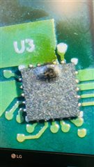
 

We would appreciate any help to resolve this issue.

Regards,

Ajay

  • Hi Ajay,

    Could you please share your schematic and layout for us to review?

    Does the circuit perform well with 3.3V output or directly damage after power up?

  • Hi Athos,

    Thanks for your reply.

    The snapshot of the schematics and layout is attached for your reference.

    The 3V3 power supply works and then randomly blows up the IC.

    Regards,

    Ajay

    3v3 Design sch and layout.docx

  • Hi Ajay,

    The schematic looks good. Please add some more information.

    • What’s the 3.3V loading actually on the board? Does it have transient process?
    • Production stage of failure application: PP stage? Early ramp? Mass production?
    • Application related questions: New project/application or old one? Is the device used for other module/project w/o issue? Is the device used on several locations or only one?
    • Production fail rate?

    Please also test the resistance Vin to SW and SW to GND to see if the MOS are damaged.

  • Hi Athos,

    The answers to your questions is as follows:

    The typical draw from the power supply is 1.5 A and transient load may be up to 5A.

    It is a prototype stage.

    This is a new design.

    We have this issue on 3 of the 5 boards. 

    Regards,

    Ajay

  • Hi Ajay,

    we may need more information for further analysis, which needs your help. 

    1. Could you help summarize the other two IC's damage phenomenon and attach the burned out pictures.

    2. Duplicate the damaged phenomenon and capture the waveforms(VIN, Vout, SW, Iout) 

    3. Test the resistance Vin to SW and SW to GND to see if the H-side MOS or L-side MOS are damaged.

    4. You can also ship a board to me to test.

    Any questions, pls let me know.

    xueliang