This thread has been locked.

If you have a related question, please click the "Ask a related question" button in the top right corner. The newly created question will be automatically linked to this question.

LM5050-1: Gate driver failure: GATE pin shorted to GND

Part Number: LM5050-1

Good day!

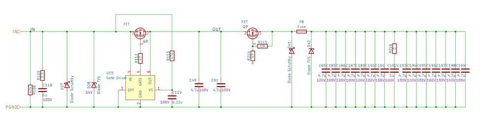
I experience high failure rates of the LM5050MK-1/NOPB driver IC and the ideal diode circuit it is used in.

The failure mode is the following: 

  • The gate driver IC fails short between GATE pin and GND pin
  • The MOSFET gate source voltage exceeds its rating (because GATE is at GND, while SOURCE is at 50V)
  • The MOSFET fails into a short between all pins
  • The ideal diode does not block anymore in reverse direction
  • The ideal diode has the MOSFET body diode drop in forward direction

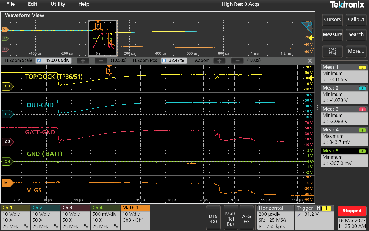
I managed to capture the following waveforms during a failure:

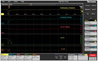
The following channels are used:

Channel 1 (yellow): IN pin of the gate driver, source of the MOSFET

Channel 2 (blue): OUT pin of the gate driver, drain of the MOSFET

Channel 3 (red): VS pin of the gate driver

Channel 4 (green): GATE pin of the gate driver

Math (orange): GATE-IN= gate-source voltage 

The following events/transients occur:

Initially, the circuit is supplied with 50V and there is basically zero load at the output side of the ideal diode circuit. There is a total capacitance of around 10uF.

Then a MOSFET connected to the output (OUT-pin) turns on to charge a large capacitive load (~60uF).

The load jump causes the voltage at the IN and OUT pins of the gate driver to fall abruptly.

The supply voltage at the VS pin remains high as there is a bypass capacitor and filter resistor present.

The IN and OUT voltages recover as the source for the circuit charges up the additional load capacitance.

However, the GATE voltage of the IC doesn't fully recover but falls to GND instead (failure of the driver IC). This kills the MOSFET.

I measured the following min./max. voltages with the oscilloscope:

IN-pin: min 4.144V, max 50.83V

OUT-pin: min 3.175V, max 50.69V

VS-pin: min 42.52V, max 50.8V

GATE-pin: min -490.6mV, max 52.72V

Based on the waveforms and minimum and maximum voltages, it is not clear to me why the IC dies.

What is the most likely cause for the failure?

Possible causes that I can think of are:

  • Negative voltage at the gate pin
  • negative voltage at another pin that is not captured by the scope
  • high dv/dt
  • high differential votlage between VS pin and IN/OUT pin

What do you think kills the IC?

Thanks for you help!

Manuel

  • Hi Manuel,

    Please share schematics for review.

    Is the output capacitor addition the only test you have performed ? This is to confirm if the IC failed during this test only.

  • I copy pasted the relevant parts of the schematics together from different schematic sheets. That's why there is no gate driver drawn for FET Q9. In the actual circuit it is controlled by an LTC7001 high side gate driver with charge pump.

    The IN-net on the left side is supplied via a ~3m cable with a 50V, 8A constant voltage, constant current source.

    Initially, we experienced 4 failures of this circuit, where we could not determine when exactly the circuit was damaged.

    Afterwards I could reproduce the failure 2 times while taking measurements. The behavior in both instances was the same and is shown in the scope screenshot I sent earlier.

    Based on these two failures, I expect that all 6 failures so far occurred during the transition I described above (this is an assumption).

    I repeat here the explanation of the transition with the schematic for clarification:

    Initially, IN and OUT are at 50V, the voltage drop across the FET Q8 is in the order of 45mV, indicating that the ideal diode circuit is working properly. The FET Q9 is off and the voltage at the right side of Q9 is 0V, i.e. the big capacitor bank is discharged. Then, the FET Q9 is turned on which causes the transient that is shown in the oscilloscope screenshot above. During this transient, the gate driver U15 fails such that GATE is shorted to GND. Afterwards the voltage drop across the FET Q8 is ~0.7V indicating that the ideal diode circuit is not working anymore.

    Some additional notes:

    • The MOSFET Q8 is SQM50020EL_GE3 or SUM60020E-GE3, we experienced failures with both of them
    • The initial 4 failures of the circuit had R113=47Ohm and C119=1uF, the first reproduction of the failure had R113=470Ohm, C119=0.22uF and the second reproduction had  R113=470Ohm, C119=1uF. I do not see any connection between the choice of components and the failure I described above.
    • For second reproduction of the failure, I had R112=10kOhm (gate resistor) and added a bidirectional TVS diode between gate and source of the FET Q8 to limit the gate-source voltage. This protected the MOSFET: i.e. only the gate driver U15 failed, but the MOSFET is still intact. Note: the first 4 failures and the 1 reproduction of the failure happened with 47Ohm gate resistor and no TVS diode and these changes don't seem to affect the failure mode of U15. From these experiments I conclude that it is indeed the gate driver U15 that fails and no other component.
    • The first 4+1 failures happened with PCBAs that were reflow soldered by our EMS, whereas the last failure was observed on a PCB that I soldered by hand with a gate driver U15 from a different source. Therefore, I think that the failure is not related to soldering/manufacturing or a faulty batch of components.

    To summarize: From my point of view the cause for the failures must be visible on the oscilloscope screenshot above. However, looking at the absolute maximum ratings from the datasheet, I cannot find any clear indication as to what precisely is the problem.

  • Hi Manuel,

    Thanks for sharing requested information. Let me review and get back to you.

  • I could reproduce the failure once more and take some better measurements.

    Initially I triggered the transient 3 times or so and the part did not fail. Then I heated the PCB/IC with a heat gun to approx. 70°C and triggered another transient and the part failed immediately. 

    Channel 1 is the voltage at the IN pin of the gate driver referenced to system ground.

    Channels 2 and 3 in this screen shot use differential probes to measure the voltages directly at the gate driver. (i.e. referenced to GND pin of gate driver) 

    Channel 4 measures the voltage of the ground next to the IC (GND) compared to the system ground (-BATT). This system ground is the reference for Channel 1.

    In these measurements, negative voltage is visible at the IN, OUT and GATE pins of the gate driver. This could be the cause for the failure. 

    However, I am not sure how this relates to 1) the apparent temperature dependency and 2) the fact that the gate driver only fails 100us after the negative voltage. 

    Another thing that I don't fully understand is the "glitchy" IN voltage at the instant when the gate voltage starts to drop due to the gate driver failure.

  • Hi Manuel,

    The device is failing as the minimum voltage rating of the device is being violated  when an additional capacitance is connected at the output. 

    To resolve this issue,

    • Introduce inrush current control for reducing di/dt while charging the additional output capacitor. This will reduce the drop in input and output voltage to within the Absolute Maximum Rating of the IC
    • Add Schottky at the input which is capable of clamping the input voltage to within -0.8V during  charging the additional output capacitor.
    • Add a diode in the GND path (D3) of LM5050-1 as shown below. This will protect the controller from input negative voltages.
  • Thanks a lot for the explanation and the possible solutions! Have a great day!