Other Parts Discussed in Thread: TUSB1146
Hi, are the design files available for this EVM please? We have Altium CAD here, it would be great if yours were in that!
This thread has been locked.
If you have a related question, please click the "Ask a related question" button in the top right corner. The newly created question will be automatically linked to this question.
Hi, are the design files available for this EVM please? We have Altium CAD here, it would be great if yours were in that!
Hi,
I sent you the board file in a private message, would you please check and see if you receive them? Unfortunately we only have the file available in Allegro format, but you can convert to Altium using this link, https://www.altium.com/documentation/altium-designer/allegro-import.
Thanks
David
Hi David, got the Allegro files OK thanks. Actually we also have that CAD system for our legacy products so can easily import to Altium. I have a couple of questions. 1 is, in addition t the datasheet I found online for the chip, is there a programmers' guide that fully explains the I2C register addresses and bit functions should we wish to implement I2C management of the device and 2. Do you know whether we would be permitted to reverse (pos-neg swap) the TX.RX SS pairs to the USB connector in order to ease PCB layout? I know you can do this for straight USB3 usage but not so sure whether it's permitted in the case that the multiplexer is delivering DP signals to these pins. I guess I'm asking whether DP pairs can be reversed which is perhaps a little off-topic for your IC :)
Hi,
Questions. 1 is, in addition t the datasheet I found online for the chip, is there a programmers' guide that fully explains the I2C register addresses and bit functions should we wish to implement I2C management of the device
Please see this app note from our PD controller team, https://www.ti.com/lit/an/slvae18/slvae18.pdf. I can also provide additional guideline on the usage of I2C registers.
2. Do you know whether we would be permitted to reverse (pos-neg swap) the TX.RX SS pairs to the USB connector in order to ease PCB layout? I know you can do this for straight USB3 usage but not so sure whether it's permitted in the case that the multiplexer is delivering DP signals to these pins. I guess I'm asking whether DP pairs can be reversed which is perhaps a little off-topic for your IC :)
No, the DP Alt Mode over Type-C spec defines the mapping of DP lane order and polarity to the USB Type-C connector called Assignment. Swapping the polarity will violate the spec definition.
Thanks
David
Hi David & thank you again. 1. The pdf in the link is more about the controller IC. What I can't find (I may just be inept!) is the I2C address of the registers within the TUSB1146, in the event that we want to use I2C to configure it. The data sheet is confusing (to me anyway) as it doesn't seem to say what its I2C address actually is. It may be buried in there somewhere, and I apologise if I have missed it. 2. Re. data reversal, OK I understand that the DP spec is the spec. But is the TUSB1146 agnostic within itself? i.e. provided all the relevant INPUTS are reversed as well as the Tx/Rx SS outputs does it matter? I'm just trying to make the routing as flexible as possible. We have a very small board area to cram all this into, as it's an upgrade to an existing product and the PCB outline is fixed. Kind regards, Laurence
Hi, Laurence
TUSB1146 I2C mode is enabled by the I2C_EN pin. It can support 1.8V or 3.3V I2C. Please see table below for the 1.8V or 3.3V I2C configuration condition.

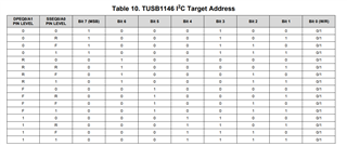
The I2C address is set by the DPEQ0 and SSEQ0 as shown below and you have 16 possible I2C address to choose. The address is a 7-bit address so you add a '0' in front of bit 7. For example, DPEQ0 = 0 and SSEQ0 = 0 will give you an address of 0x01000100 which is 0x44h.

For the polarity, if both the DP input and output lane polarity, then I do not see an issue.
Thanks
David