This thread has been locked.

If you have a related question, please click the "Ask a related question" button in the top right corner. The newly created question will be automatically linked to this question.

ucc3895 application question

Other Parts Discussed in Thread: UCC3895, UCC28950

Mike,

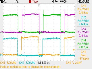
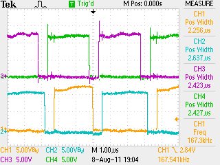
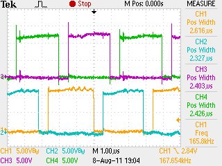
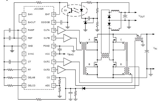
Our customer Emerson using our ucc3895 and add some external circuit for the phase shifted full bridge synchronous rectifier ,they find the OUTA positive duty cycle have a little difference to OUTD ,OUTB and out OUTC also have the same phenomenon,

There difference is about 300ns at 65kHz operation frequency. That means that the OUTD may have 300ns more positive duty cycle than OUTA each period. Is this phenomenon reasonable? Customer told me this issue only happens at close loop. There is no problem at open loop.

Emerson want us give one training about the phase shifted full bridge application to them, including the main topology and design tips and consideration, and simulation. Do you have any material about the phase shifted full bridge can share to me?


Best Regards

Swing Jiang

  • Hello Jiang,


    In peak current mode control designs I have seen duty cycle jitter of about 200ns.

    This was because the transformer turns ratio of the power stage is not exact. 

    This is documented in the UCC28950 user’s guide which can be found at the following link.

    http://focus.ti.com/general/docs/lit/getliterature.tsp?literatureNumber=sluu421a&fileType=pdf

    Please look at figure 21 and 22.  Power stage schematic is in figure 1.


    If the design is peak current mode control the difference in duty cycle is just correcting for the mismatch in the transformers turns ratio primary to secondary.


    Regards,


    Mike

  • Hello Mike,

    I also have the same problem here.

    UCC3895 is configured as voltage mode.

    A resistor from Vref to RAMP (Pin3) and capacitor from RAMP to GND.

    CS (Pin12) is not yet connected to the CS of the sense resistor.

    Here are the waveforms I get.

     OPEN LOOP


    Ch1 = OutC (Pin14)

    Ch2 = OutD (Pin13)

    Ch3 = OutA (Pin18)

    Ch4 = OutB (Pin17)

    CLOSED LOOP (NO LOAD)


    CLOSED LOOP 1/4 LOAD

    Here is the basic sch i made except for RAMP resistor to REF pin.

    The ill effect will be for the pulse transformer being not balanced due to different volt-second for OUTC and OUTD.

     Victor