


Like Shyama, I had some false turn-on of the PDSG FET. Using his circuit, our FET has a Vgs(min) of -2V. To develop that voltage at Vgs, we only need 2uA of leakage through the 1Mohm RGS1.
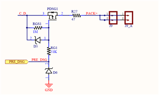
This leakage could be through D6 to ground or sunk into the BQ76952 PDSG pin. Figure 1-10. PDSG Pin Equivalent Diagram in sluaaf2.pdf shows the leakage paths.
Can TI advise the leakage into that pin at say 85degC ?
For now, I also had a 75V protection zener (D6) for the PDSG pin; an On Semi MMSZ5267BT1G. The On Semi datasheet has a flat reverse leakage current of 0.08uA @ 150degC (see Figure 8. Typical Leakage Current).
So to calculate a value for RGS1 with some margin (say Vgs @ 1V for circuit leakage at 85degC), the leakage into the PDSG pin seems to be the one I need to consider.
RGS1 and RG1 then have to not exceed the sink current for the PDSG pin which the BQ76952 datasheet specifies as typically 30uA; see "7.8 Precharge (PCHG) and Predischarge (PDSG) FET Drive"
In "11.5.2 PRECHARGE and PREDISCHARGE Modes", the datasheet suggests "The PCHG and PDSG drivers are limited in the current they can sink while enabled. As such, it is recommended to use 1 MΩ or larger resistance across the FET gate-source." but I am not sure this is right for my situation. I don't want to simply replace the 1Mohm with 500kohm without understanding the behaviour.
I have tried to find a PDSG leakage value in the data. Apologies if I missed it but I also need this at 85degC since resistors for pack reverse voltage protection will be heating adjacent to the BQ76952. I want the board to maintain protection for a sustained voltage reversal.
All the best
Harry

