A related question is a question created from another question. When the related question is created, it will be automatically linked to the original question.
If you have a related question, please click the "Ask a related question" button in the top right corner. The newly created question will be automatically linked to this question.
TPS630250: input side shorted and output is partially shorted as well
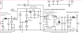
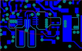
The input side pin 4-10 shorted to ground and output is partially shorted as well. It is not a hard failure, It failed between 0.5H to 2 hours. Below is schematic and layout
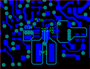
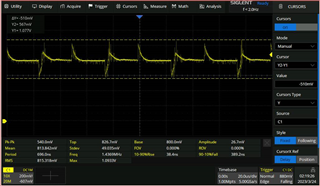
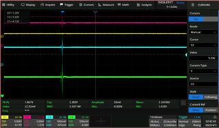
Our application has a BLDC motor involved. Three motor wires run through the top of this chip. I captured the Feedback signals between motor wires close or a little far away from TPS630250.
Also, we got this design from WBENCH tool. The voltage divider resistance is pretty large. We are wondering if we can change them to 4.7K and 1.5K? Any risk to do it. Our application needs 1.5A in the most of time. Thank you.
The only concern you change the resister divider to smaller one should be the high consumption, if it is acceptable, i think it is should be ok.
i am afraid the root cause is not the disturbed FB, what is the actual input voltage in your APP? i suspect the damaged device is caused by the high volltage at node Vin, Vin+spikes.
Tao, thanks for your reply. For the smaller resister divider, you mentioned it would introduce high consumption. Is there any thermal concern? For our application, the normal input voltage is 4.0v or 5V. I checked the input voltage, no very spike found, under 5.5V. The 5v is from another DC-DC buck converter and 4V is from a big charged capacitor.
Was this chip switching between buck and boost mode?
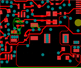
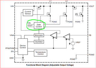
I guess the gate control ( in green circle) is the one that decides to run as buck or boost.
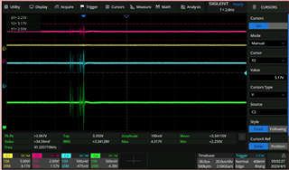
On one of our failure board, I removed L203 and check impedance for L1 and L2. The L2 to ground is zero, and L1 to ground is 283.5K. Does it mean that the chip was running as boost mode sometime?
if the input voltage is 4-5V and output is 3.3V, i think device will always work in buck mode. although there is a diode in series between power input and your board. Device should not work in pure boost mode. so I am confused about the attached picture.
Mode transition of this device is not only depend on the voltage, also the output current. But, yes, you can almost think it is depend on voltage only.
i still think the high risk should be the voltage out of spec in you Vin and L1 pin.
At the beginning, the motor was spinning. then motor stopped, so the noise/switch was gone. The motor wires were on the top of the IC203 (this buck-boost coveter
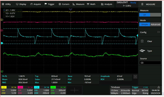
I found an interesting during I switched battery. We have a big cap (charged to 4.5v) in place which functions as an temp power supply so the system is not shut down for 15 seconds. The operator can change battery during the 15s. There are a quick transient on 3.3v output line that is higher than 4v. I am wondering if such high voltage transient will kill the internal output MOSFET?
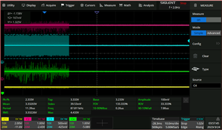
Do you know why the output transient to higher than 4V? i think it should be stable at 3.3V because the feedback divider is a fixed one and will not change during this power switching, right?
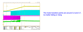
For 3.3V output, the mode transition point should be similar as below. if the ouput is higher than 4V, yes, the device will work in boost mode.
Rong has shared the design files with me and I have just sent it to you directly for further review in order to comment on improvements that can be made in the layout and schematic.
Feel free to share your design review feedback to me and I will be sure to pass it along to Rong.