


Dear Sir/Mam
I develop UCC2897A as ACF Converter, with the following specifications:
Vin 60Vdc-90Vdc
Vout 12V
IOut 7A
Fsw 200KHz
Np : Ns 15 : 6 (2.5)
Lp 300uH
Llkg 1uH
Lout : 22uH
Secondary rectifier : Schottky diode SDT10A100P5 (1st board) and Mosfet BSZ146N10LS5 (2nd
I have a major technical issue with both board :
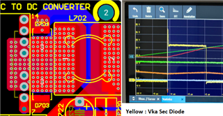
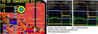
1. Vka (or Vds in SyncRect case) waveform, have very big overshoot, even the PCB trace between diode - Secondary coil and Secondary Inductor are very short. You can see at the attached picture, they are very close to each other, and the Vka waveform is in yellow. I use 1.5 damping factor for the snubber)
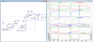
2. I do simulation using LTSpice , if the primary and secondary coupling is 1, then there is no issue with the Vka waveform, but when i use 0.995 as the coupling factor, the overshoot become very terrible, then i add RC snubber with damping factor 1 and even 2, the overshoot still visible, it will not disappear completely., the first (in case oh schottky diode) and up to third (in case of mosfet sync rect) oscilation still visible.
My question are, in the UCC2897A EVM test report.and other UCC2897A ref design report, even there is no RC Snubber at the secondary rectifier, there is no overshoot with Vka or Vds waveform, how can it be? Why i can't make a clear waveform with my board or even in LTSpice simulation if the leakage inductance is present as in the EVM or TI's Ref design ?


Thank you and best regards
evan
