Need to Trigger MOSFET at 48V for a Source switching circuit, can you help. THe primary source should be feeding the load and the failure of primary should switch the auxilary source.
This thread has been locked.
If you have a related question, please click the "Ask a related question" button in the top right corner. The newly created question will be automatically linked to this question.
Need to Trigger MOSFET at 48V for a Source switching circuit, can you help. THe primary source should be feeding the load and the failure of primary should switch the auxilary source.
Hi Suhas,
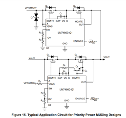
LM7480-Q1 would be right device to achieve Priority Power Muxing. You need to use 2x LM7480-Q1 to drive back-to-back FETs in each power path to realize Priortiy Power Muxing as shown below.
For more understanding on this circuit, please refer to section 'Design # 6: Reverse Battery Protection With Priority Power MUXing' of Six System Architectures With Robust Reverse Battery Protection Using an Ideal Diode Controller Application note.
Can i control it through a micro controller , also regarding the Resistance values i need some clarification
Hi Suhas,
In the above circuit, the switch over from PRIMARY to AUXILIARY rail is automatic. If required you can control it through Micro Controller as well.
I would recommend you to use the OV pin to turn ON/OFF the power path rather than using the EN/UVLO pin. This is because when the EN/UVLO pin is pulled low, the charge pump is disabled and when the EN/UVLO pin is pulled high there will be delay for the HGATE to turn ON as the charge pump turn ON takes time.
This delay will not be present when OV pin is used because when OV is pulled high only the HGATE is pulled low turning OFF the power path where as the charge pump remains ON and hence when the OV is pulled low the HGATE is turned ON immediately without any delay.
Can you elaborate on your question regarding the Resistance values ?
i was asking about the Resistance values r1, r2, r3 and r4, in the circuit. that is in the network of sw and OV.
So what u are suggesting is to connect the micro controller to the OV pin and trigger
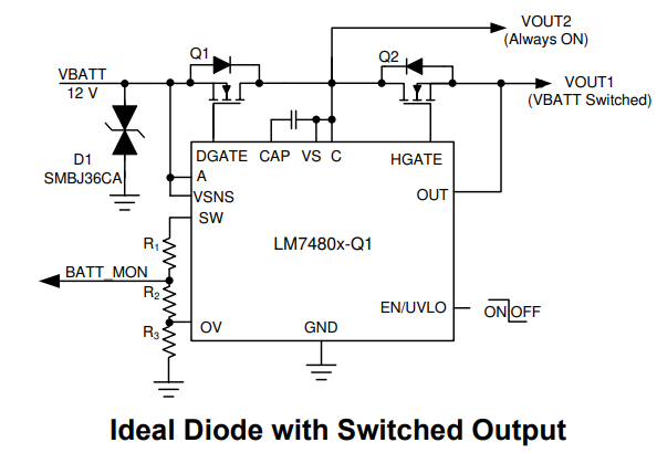
R1 and R2 can be calculated depending on over voltage protection threshold on VPRIMARY and V(OVR). Say for example, You want VPRIMARY OV protection at 16V then R1 and R2 resistor ladder components should be selected such that when VPRIMARY is 16V the voltage seen on the OV pin is at V(OVR) = 1.231V
The components R6, R3 and R4 can be calculated depending on the VPRIMARY to VAUX transition. For Example, you want to transition from VPRIMARY to VAUX when the VPRIMARY falls below 8V, then the R6, R3 and R4 needs to be calculated such that when VPRIMARY = 8V the voltage seen on the OV pin is V(OVF) = 1.1.3V
my higher voltage is 60V and Lower Voltage is 35V.. How do i control it through Micro controller
I want a circuit that would work as follows.
The primary source should be connected at all times, when the primary fails the secondary should kick in, After this even if the primary starts back again it should not go back to the primary.
Are there any circuit that could help this work
The Microcontroller control signal outputs can be connected to OV pins of LM7480-Q1 in both the rails. This way you can control the turn ON and turn OFF of each power path by pulling the OV pin HIGH or LOW respectively.
where should i connect the Sw pin then, On TINA i am not able to do a proper Simulation
Hi Suhas,
Please click each of the warnings and resolve them before simulating. Looks like there are a few open connections.
this seems to be working But just a doubt, why is the lower IC works without a trigger from the Micro controller
The lower IC (U4) is working because the OV pin is connected to GND. In case you want to verify its operation with microcontroller control signal, use a voltage source at OV pin similar to one used at OV pin of U1.
5857.LM7480Q1 ORing.TSC can i connect the MOSFETS in Parallel as shown in the Schematic..
Hi Suhas,
Please refer to the datasheet description section to understand the conditions during which HGATE and DGATE are ON/OFF.
For Priority power Muxing application, you can use any of the devices - LM74800-Q1 , LM74801-Q1 or LM74810-Q1
I am not able to Find the other online, Only LM74810-Q1 is in stock , can i use this for the same schematic
All these devices (LM74800-Q1 , LM74801-Q1 or LM74810-Q1) are pin-to-pin and can be used interchangeably.
Yes, you can use LM74801-Q1 IC by ordering from the above links.
Hi Suhas,
1. The Orientation of Diode FET (T2, T6, T4, T8) is wrong. Reveres the FET Drain and Source connections, i.e. connect Source of the FET to the input. The correct FET connections are as shown below.
2. If the internal disconnect switch between VSNS and SW is not used then short them together and connect to VS pin.
3. The OV pin of LM7480-Q1 is connected to GND which means U2 is always ON (related to OV). Please check if this connection is okay for you.
LM7480Q1 ORing (1).TSC I was using this as the reference of what u had given earlier. But now i checked again if u2 supply is higher then this supply will be connected to the output we dont need that. I want to control each suppy individually. I have added a seperate signal to OV, which still doesnt solve my case
Hi Suhas,
Thanks for your response. Let me review and get back to you within couple of days.
Hello Praveen GD>
We got this PCB ready. It works fine with 24V Motors and sources. But when i use a 48V system the IC heats up and the MOSFET get damaged. as soon as the it is triggered the first time.
The TINA simulation file schematic looks okay to me. Can you share the actual schematic of your board ?
Hi Suhas,
the schematic connections look okay to me except for the input TVS diodes. Can you elaborate the test condition during which the IC/ FETs fails. Also please share with me waveform captures during startup the condition which the FET/ IC fails. Please capture, VIN, VS, VCAP, HGATE, DGATE, VOUT signals.
Hi Suhas,
With high output capacitance, the current flow during startup will be very high. This can cause FET SOA violation and damage to the FET.
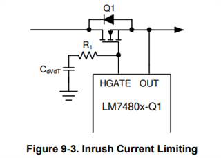
Here, you will have to use dvdt based startup for inrush current control. Select Cdvdt such that the inrush current during startup (calculated using the below formulae) is within FET SOA.
Hello Praveen GD i used this Formulae. calculated with Ihgate_drv as 55uA, Inrush as 30A and Cout as 2500uF. the Cdv/dT i got was close to 4700pF,
i used a 4700pF capacitor in series with a 1k Resistor.
the issue still persists. Just see if my calculations were correct.
Hi Suhas,
30A inrush is Huge. You need to reduce the inrush current which the FET can handle with VDS of Vin across it. Please follow the below steps to check if the FET selected has good SOA margin for the selected Cdvdt. I would recommend to start with a Cdvdt of around 100nF.
FET SOA stress calculation
A more detailed explanation of SOA calculation is specified in section 2.3 Understanding MOSFET’s Stress Limitations of Robust Hot Swap Design App note.
For your understanding below is a step by step procedure (extracted from the app note),
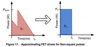
1. Calculate the power stress on the FET during startup. Refer to section ‘2.3.3 Checking SOA for Non-Square Power Pulses’ of the app note.
Derive t2. Approximation here is that the FET is stressed for a power loss = P2 = PMAX for t2 duration.
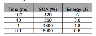
2. Now, estimate SOA the FET can handle for t2 duration. This value will be at room temperature. Refer to section ‘2.3.2 Checking SOA for Intermediate Time Intervals’ of the app note.
Remember that the SOA value in the table below needs to be taken at VDS = VIN(max) in the SOA curve of the FET.
3. Now, De-rate the SOA calculated in the above step for the Max operating junction/ case temperature of the FET. Refer to section ‘2.3.1 MOSFET SOA Curve and Thermal Model’ of the app note.
This value can be taken as the temp. of the FET at max load condition,
4.You can consider that the FET has strong SOA if
SOA(TC) > 1.2 x (P2 / VDS)
Where,
SOA(Tc) is from step 3
P2 is from step 1
VDS = VIN(max)
The factor 1.2 is taken to include a 20% margin.