This thread has been locked.

If you have a related question, please click the "Ask a related question" button in the top right corner. The newly created question will be automatically linked to this question.

TPS3422: Latched switch not working as expected, board is getting hot

Part Number: TPS3422
Other Parts Discussed in Thread: SN74LVC1G74, STRIKE

Hi,

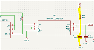
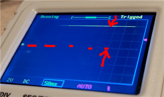
I have designed latched switch using TPS3422EGDRYR and SN74LVC1G74DQER. Schematics of this design is given as below. Input supply is 5 V. It works while in open load condition and show 5 V as output, but as soon as I connect main circuit with this board it drops the voltage. I noticed SN74LVC1G74DQER is getting hot. 

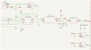
Can someone please suggest what could be wrong? I went through the schematics but could not find any issue.

  • Hi Gaurang,

    Where is the load being applied too?

    Jesse 

  • Hi Jesse, Load is connected with connector J70 and J73.

  • Hi Gaurang,

    I am currently still looking in this. I will give you an update soon.

    Jesse 

  • Hi Gaurang,

    The only concerning part of your schematic that I can see is the R70 is only 1kohm. I would typically recommend for the pull-up resistor of an open drain be at least 10kohm. Other than that the TPS3422 schematic looks fine. Since the load is interfaced through the BGA, I would recommend checking the current of PIN 5 of the SN74.

    Jesse  

  • Hi Jesse,

    Thanks for the suggestion.

    So far, I have tried following:

    1. I replaced R70 as you suggested with 10k resistor. it did not worked. heating issue is still there.

    2. I replaced fuse with 1k resistor, it didn't worked

    I observed following things.

    1. Board is consuming current in the range of 800mA, which seems to be reason for heating, it wasn't possible to measure exact current on the pin 5 of SN74 due to complex design.

    2. I also observed that resettable Fuse is getting hot as well due to increased current. As a result I am only getting 750 mV on the load side. 

    Please let me know if you have any other suggestions.

    Thanks,

    Gaurang.

  • Hi Emrys,

    Could you please help Gaurang do his issue analysis from the SN74LVC1G74 perspective? I do not see any issues on the TPS3422 side.

    Jesse 

  • Hi Gaurang,

    With 800mA of unexpected current, I highly doubt that the SN74LVC1G74 is the primary issue. It is possible that it was damaged and has become a short -- is this happening in multiple boards?

    The 'LVC1G74 is a CMOS device, so the inputs must be fast transitioning -- the RC at the CLR\ input could result in damage to the device:

    This type of damage is fairly uncommon though, so if you are seeing this in multiple boards, it is probably coming from a different source.

    If you want to update your design to avoid this entirely, the appropriate method to provide the power-on reset is shown in this short video: Generate a Reset Signal at System Power On | Video | TI.com 

    -

    Can you get scope shots of the CLK input and output (Q) of the 'LVC1G74?

  • Hi Emrys,

    There are few observation I've made which led me to believe that SN74LVC1G74 is not getting damaged. 

    1. When there is no load connected on board, LED power on and off as expected. Problem arise only when there is significant load connected and fuse starts getting hot.

    2. If you bypass the fuse, SN74LVC1G74 gets hot. But works well if load is disconnected and only LED is connected as a load.

    3. Due to complex pcb design, I could not take scope shot of mentioned signals.

  • I cannot troubleshoot with you unless you can get the waveforms -- these are critical to determine what is going wrong, if anything.

  • Hi Emrys,

    1. I have taken snapshot of input clock signal for 'LVC1G74 as you requested. Please take a look, it seems normal to me.

    Switch-Turn onSwitch - Turn off

    2. To take the snap of signal on the output(Q) I removed U72 from PCB and probe oscilloscope on B2 pad of U72. I'm getting good signals

  • The time scale is absolutely huge -- these devices operate on the nanosecond scale. What I'm looking for is a discernible edge rate at the input that is faster than the requirement in the datasheet:

    From your video:

    I see that the output is offset by about 1V from the ground reference. This would indicate a large amount of current flowing into the output of the device when it is in the low state. From the datasheet:

    The worst-case V_OL is 0.55V with 32mA of current at 4.5V supply. This indicates a maximum resistance at the output of about 17 ohms.

    Typically the value is lower - closer to 10 ohms. Assuming you have a typical device, the output current is around 100 mA, which is in violation of the datasheet maximum output current.

    -

    There is another possibility - if the output were damaged due to something like an ESD strike, the drive strength at the output could have been affected. I don't believe this is the case though considering the output signal is also clamping on the positive voltage side:

    It looks to me like something is trying to pull the output up beyond the operating voltage range of the device, and the output is clamping that voltage.

    -

    What is the load connected to this output?