This thread has been locked.

If you have a related question, please click the "Ask a related question" button in the top right corner. The newly created question will be automatically linked to this question.

TPS25750: TPS25750S connection

Part Number: TPS25750
Other Parts Discussed in Thread: TPS65987D

Hello, I plan to use the TPS25750S in this way, with it acting as a downstream-facing port data wise, and a DRP port power-wise depending on the situation:

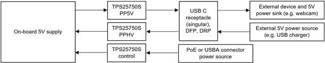
Basically, the idea is the board is powered by:

  1. External USB C receptacle
  2. PoE solution
  3. Internal USB A receptacle

In the listed priority order. In addition, when a power supply is not plugged into the USB C receptacle, a device can be plugged into it which will be powered by the board.

A TPS25750S GPIO pin will be connected to the enable pins of the other power sources to deactivate them when the TPS25750S PPHV power path is enabled.

Is this an acceptable way of implementing this?

  • Good Morning Aria,

    I will review your implementation and provide feedback by 4/3 EOB.

    Kind regards,

    Conner Gillette

  • The PPHV power path on the TPS25750S is not integrated, while PPHV is integrated in the TPS25750D. If you use the TPS25750S for your design, you will need an external NMOS, for switching PPHV. The TPS25750 datasheet has an example schematic and part.

    Since you're only using PPHV for sinking, you can use the AttachedAsSink GPIO event, or you can read the 0x26 POWER_PATH_STATUS register directly.

    I see no issues with your implementation based on your block diagram.

    Kind regards,

    Conner Gillette

  • Thank you for the assistance, however, I've decided to use the TPS65987D instead as it allows integration with a DP/HDMI mux, which I will use to switch HDMI signals. I will open a separate question.