This thread has been locked.

If you have a related question, please click the "Ask a related question" button in the top right corner. The newly created question will be automatically linked to this question.

TPS2121: Output drop occurs when switching between IN1 and IN2

Part Number: TPS2121

Hello,

I am an FAE for a distributor that handles TI products.
I have received inquiries from customers about the TPS2121.
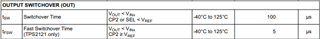
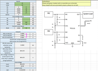
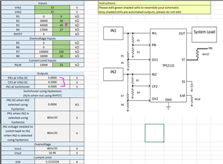
In the customer's circuit, the input switching mode uses XREF, and the ST pin is used as a status signal instead of hysteresis.
Both IN1 and IN2 are 12V.
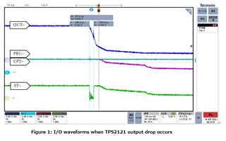
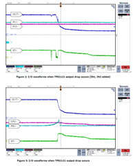
The symptom in question is that the output voltage drops by about 25ms when switching from IN1 to IN2.
This is a similar symptom to the thread below, and I'm assuming the same is happening in my customer's circuit.
(Question 1)
In the thread below, it seems that the output is dropping due to the occurrence of bounce near the reference voltage.
Is output drop the only symptom caused by this bounce?
Also, what is the assumed cause of the output drop?
Is the internal Nch-MOSFET malfunctioning?
Are there any other symptoms after that?
(Question 2)
How fast should the comparison signal be switched with respect to the reference voltage so that the bounce does not cause an output drop?
Please let me know if there is a recommended value for the time for the comparison signal to change.

Best regards,

e2e.ti.com/.../tps2121-output-voltage-dropout-during-switchover
https://e2e.ti.com/support/power-management-group/power-management/f/power-management-forum/1064834/tps2121-fast-switchover-time?tisearch=e2e-sitesearch&keymatch=tps2121

  • Additional information.
    After the output drops, IN1 is output instead of IN2.
    Since CP2>VREF and CP2>PR1, IN2 should be output.
    If the output drops, is it expected to be in the above situation?
    Best regards,

  • Hello, 

    Could you provide a schematic and scopeshots of this issue to confirm?

    However, yes this is likely an issue of multiple switchovers between both inputs. The power mux device is always responding to its inputs. During fast switchover, there is no soft start or current clamping. Therefore, when the device switches from one supply to another, the unselected supply will rise slightly in voltage as the source is unloaded while the loaded supply will slightly drop in voltage as current is being drawn. Since a switchover event occurs when CP2 and PR1 intersect, it is possible for the device to bounce between the inputs during this switchover point as the voltage of each chosen input drops while the other raises. The PR1 and CP2 comparator is quite sensitive which could cause a change the PR1 and CP2 comparison over and over again, especially so if the Vin rail is not stable.

    To solve this, I would recommend adding a hysteresis resistor between ST and PR1 further detailed in the following FAQ: https://e2e.ti.com/support/power-management-group/power-management/f/power-management-forum/1023453/faq-tps2121-how-do-i-achieve-a-seamless-power-switchover-using-ti-s-power-mux-devices

    At the bottom of this FAQ is a excel calculator tool which can be used to better understand the switchover point based on your voltage divider and the impact of hysteresis on your switchover voltage back to IN1 after IN2 is selected. 

    The symptoms here are going to be an output voltage drop several switchovers. 

    Best Regards, 

    Elizabeth 

  • Thank you for your reply.
    See if the customer can share the schematics and waveforms with you.
    I would like to ask you again about what you have stated at the end.
    Can you explain the principle why the output voltage drops after switching several times?
    Best regards,

  • Hello,

    I am attaching the schematic and waveform.
    Supplement the operation of the schematic.
    A regulator is used behind MUX_OUT to generate DC +5V.
    2V is created by resistance division from DC+5V and applied to CP2.
    After +24V DC, a buck converter is used to generate +12V DC.
    IN1 is input first, and when DC+24V is input, the PNP transistor turns off, PR1 decreases, and the input switches to IN2.

    Currently, it occurs only in the inspection process before shipment, but we believe that it may occur in the market where the product is shipped.
    Therefore, we need to understand what mechanism causes the output drop.
    We've seen similar drops in past E2Es, so I think you know the mechanism.
    Please let me know your opinion on this.

    Best regards,

    8507.schematic.pdf

    Description of waveforms and symptoms.pdf

  • Hello, 

    Our TI power muxes work in a break-before-make configuration. This means once the device decides to switch from one input powering the output to the other, the device will disconnect both input paths to the output. After tsw time, the device will then reconnect the other path from the secondary supply to the output. During this tsw time, no input is connected to the output so the output voltage will fall. 

    To determine if the customer is experiencing this phenomenon as described in the following FAQ: https://e2e.ti.com/support/power-management-group/power-management/f/power-management-forum/1023453/faq-tps2121-how-do-i-achieve-a-seamless-power-switchover-using-ti-s-power-mux-devices where the device is switching from one supply to the other, the customer could probe the ST pin at 10us/div to see this behavior. 

    By the look of the scope shots provided, it appears this voltage drop is occurring when PR1=CP2 as expected if this were to be a drop in voltage due to a switchover event. This can be confirmed by overlaying the PR1 and CP2 scope shots to the same potential to see if they intercept when the output drops in voltage.

    Since you OVx pins are greater than VREF and the current limit is not triggered, this is not likely a fault trigger. 

    Best Regards, 

    Elizabeth 

  • Thank you for your reply.
    You said that you could identify the cause by checking the waveform of the ST pin in as short a time as possible, so the customer measured the waveform again.
    I am attaching the waveform.
    The customer intentionally made the fall of PR1 slower and measured.
    This is to make this phenomenon more likely to occur.
    As a result, as shown in the attached waveform, the ST pin output bounced many times within a short time of less than 1 ms.
    In addition, OUT is also unstable accordingly.
    In this measurement, it is a symptom in which OUT fluctuates in an unstable manner over a period of tens to hundreds of μs.
    It's not the drop in OUT over the tens of ms of the waveform provided earlier.
    (Question)
    In such a state where ST bounces repeatedly, is there a possibility that OUT will drop in a few tens of ms?
    Best regards,

    ST and OUT waveform.pdf

  • Hello, 

    Thank you for the provided waveform. 

    As evident by the ST plot, the device is switching between selecting IN1 and IN2 to power the output. 

    To reiterate, our TI power muxes work in a break-before-make configuration. This means once the device decides to switch from one input powering the output to the other, the device will disconnect both input paths to the output. After tsw time, the device will then reconnect the other path from the secondary supply to the output. During this tsw time, no input is connected to the output so the output voltage will fall. 

    Therefore, whenever ST changes states, we should expect a drop in the output voltage for (tsw seconds). If this switchover continues, we should expect a drop in output voltage for (tsw seconds * the amount of switchovers occurring). 

    To address this, I would recommend adding a hysteresis resistor between ST and PR1 further detailed in the following FAQ: https://e2e.ti.com/support/power-management-group/power-management/f/power-management-forum/1023453/faq-tps2121-how-do-i-achieve-a-seamless-power-switchover-using-ti-s-power-mux-devices

    Best Regards, 

    Elizabeth 

  • Thank you for your reply.

    The customer measured the average bounce time in the customer's circuit.
    The bounce time is the time from when the ST voltage level switches until it stabilizes.
    The number of measurements is 10. Below are the results.

    220, 420, 190, 270, 320, 280, 240, 270, 260, 280 [μs]
    →Average 275 [μs]

    The average bounce time in the customer's circuit was 275 µs.
    The 20ms to 30ms voltage drop that the customer is concerned with is clearly outside the normal distribution of the average bounce time above.
    Therefore, the 20 ms to 30 ms voltage drop cannot be explained by this bounce phenomenon alone.

    However, if this bounce can cause collateral damage, it can explain the voltage drop of 20ms to 30ms.
    For example:
    Example) Due to repeated bounces, the switching of the Nch-FET inside the device between IN1/2 and OUT malfunctions.

    Could a bounce cause such collateral damage?

    If the voltage drop of 20 ms to 30 ms cannot be explained by this bounce phenomenon alone, there is a possibility that there is another factor in the customer's circuit that causes the voltage drop besides this bounce.
    Customers are very worried about it.

    Best regards,

  • Hello, 

    The device will be evaluating PR1>CP2 to determine what input to designate as the output. 

    Based on your schematic, at DC conditions the device will be attempting to determine PR1 (5V)>CP2 (4.9091V). These values are very close to each other and could result in a situation where the device switches back and forth between the two inputs. 

    This bounce will not damage the device as this device has a break-before-make configuration which ensures the inputs are never both connected to the output. Additionally, this device has a thermal shutdown feature which will disable the device when it exceeds the TSD temperature. 

    Other reasons the device could be disabled for a longer period of time could be a thermal shutdown trigger or overvoltage trigger, neither of which would harm the device. To avoid this issue, I would recommend the following schematic changes:

    • Altering your voltage divider on CP2 to add a larger differential between the PR1 comparison. For example, switching R513 to 45kohms would change the switchover voltage to 4.5V. 
    • Adding a hysteresis resistor from ST to PR1

    This is how your schematic stands currently:

    This is what I propose: 

    Do note this is not including hysteresis. Hysteresis in your schematic currently would do no good as the PR1 pin is connected directly to a 5V bias. To add hysteresis, you would need to add a R1 resistor as illustrated in the excel sheet. 

    Best Regards, 

    Elizabeth 

  • I have received additional information from the customer regarding the above, so please let me know your opinion.

    The customer measured the input and output waveforms of the TPS2121 when the output drops under the following conditions.
    ・ Added ST pin to the measurement point
    ・ Set the time axis to 1 ms/DIV
    The waveforms and their descriptions are summarized below.
    Could this waveform behavior be due to output switching bounce?
    Also, if you can think of any other suspicious factors, please let me know.

    ・The voltage drop of OUT for a long time (> 5 ms) occurs when the voltage levels of PR1 and CP2 overlap and OUT is switched. (see PR1, CP2, and ST in Figure 1)
    ・A bounce of approximately 200 μs occurs immediately after OUT switches from IN1 to IN2. (See ST in Fig. 1)
    ・In about 200 μs immediately after OUT switches from IN1 to IN2, the OUT voltage drops from about 13 V to about 8 V. This voltage is well below the IN2 voltage (approximately 12 V). (See OUT in Fig. 1)
    ・About 200 μs after OUT switches from IN1 to IN2, OUT switches from IN2 to IN1 again. (See ST in Fig. 1)
    ・Even after OUT is switched from IN2 to IN1 again, the voltage of OUT does not recover. continue to decline. (See OUT in Fig. 1)

    Best regards,

  • Hello, 

    For clarity, could you please share the schematic for when the following waveform was captured. 

    Best Regards, 

    Elizabeth

  • I am attaching the schematic.
    Supplement the operation of the schematic.
    A regulator is used behind MUX_OUT to generate DC +5V.
    2V is created by resistance division from DC+5V and applied to CP2.
    After +24V DC, a buck converter is used to generate +12V DC.
    IN1 is input first, and when DC+24V is input, the PNP transistor turns off, PR1 decreases, and the input switches to IN2.
    Best regards,

    2072.schematic.pdf

  • Hi Kaji, 

    Thank you for sending over those materials! 

    The switchover event is going to occur within 5us typical. To observe whether this voltage drop can be attributed to the constant switchovers, you would need to zoom in to ~10us/div. 

    If you do not see a switchover every ~5us, Could you also share a plot of IN1 and IN2 for the time duration the previous waveform was captured. 

    What I hope to conclude is whether the output is following either input, however I would expect to see a switchover between IN1 and IN2 powering the output every 5us resulting in a large output voltage drop. 

    Best Regards, 

    Elizabeth 

  • Thank you for your reply.
    I have attached the waveforms of IN1 and IN2 during the voltage drop you requested. This is the waveform in Figure 2.
    Both IN1 and IN2 appear to be stable before and after the voltage drop occurs.
    In addition, the customer was able to observe the waveform when the voltage drop occurred at a new timing different from before. This is the waveform in Figure 3.
    Until now, the voltage drop occurred when switching from IN1 to IN2 (timing of PR1<CP2).
    In the waveform observed this time, a voltage drop occurs when switching from IN2 to IN1 (when PR1>CP2).
    Also, as far as the ST is concerned, it seems that there is almost no bounce.
    Please let me know if the waveforms in Figures 2 and 3 are due to bounce effects.
    Best regards,

  • I understand you are very busy, but would you be able to answer my inquiry?
    Best regards,

  • Hi Kaji, 

    Apologies for the delay; I was out of office.

    I will not be able to conclude this voltage drop you've shown is due to the bounce effects at the time scale provided, however that is my suspicion. The switchover event is going to occur within 5us typical. To observe whether this voltage drop can be attributed to the constant switchovers, you would need to zoom in to ~10us/div. 

    Best Regards, 

    Elizabeth