This thread has been locked.

If you have a related question, please click the "Ask a related question" button in the top right corner. The newly created question will be automatically linked to this question.

TPS55288: Help verifying schematic and PCB layout

Part Number: TPS55288
Other Parts Discussed in Thread: TPS55289

Hello E2E Experts,

Good day.

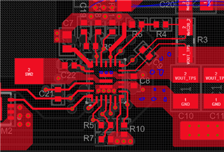
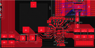
For a project, I decided to use the TPS55288 as a variable DC voltage source. I have designed a working prototype board before but it had some flaws, which is why I want to check it first. I have included the schematic file. There is some additional circuitry, but I would like some feedback on the tps55288 part of the circuit. Some information that is not on the schematic: 

Expected maximum output power: 40W

Maximum output current: 2A

Input voltage: 5 - 20V

Output voltage: 2 - 20V

Am I missing something important? I would like to optimize this design for a low-as-possible output ripple at maximum output power.

DC2DC.pdf

I will try to finish the PCB layout as well.

Regards,

CSC

  • Hi CSC,

    Please see my comments below:

    1. For this application power range, we recommend TPS55289 which is four-MOSFET integrated and is easy for design and layout.

    2. For Layout:

    (1) Recommend to add more vias at Vout and GND copper plane.

    (2) Recommend to separate AGND and PGND plane at VCC cap. And connect all signal pins ground to AGND plane.

    Regards,

    Bryce

  • Hello Bryce,

    Good day.

    I am considering using the TPS55289. I am using the Power Designer customization software from TI. I want to use an LDO to filter out a big portion of the switching noise but for this, I need the frequency to be as big as possible. When setting the frequency to 2MHz it says the design is unstable, why is this? How could I maximize the frequency while having the design be stable?

    Regards,

    CSC

  • Hi CSC,

    What is the input and output condition when you type in the Webench design? It may be because of the unsuitable compensation parameter.

    Regards,

    Bryce

  • Hello Bryce,

    Good day.

    Attached herein are the two screenshots, changing the user-preferred frequency to something like 2MHz will make the design unstable, what is the limiting factor is what I would like to know.

    Regards,

    CSC

  • Hi CSC,

    Thanks for notice here. The operation condition you input(Vin=14~16V, Vout=20V, Iout=0.5A, fsw=2MHz) is suitable for TPS55289, I think there is something wrong with Webench simulation tool and we will ask the Webench team to correct that. 

    Regards,

    Bryce