This thread has been locked.

If you have a related question, please click the "Ask a related question" button in the top right corner. The newly created question will be automatically linked to this question.

TPS2660: dVdT operation on reverse input supply connection at OVP disable condition

Guru 19645 points
Part Number: TPS2660

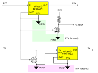
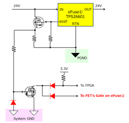
Application note: slva811a is described the solution on OVP disable from FET, please refer page 14 and attached below.

https://www.ti.com/jp/lit/an/slva811a/slva811a.pdf

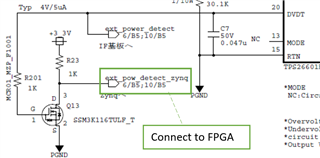
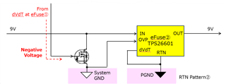
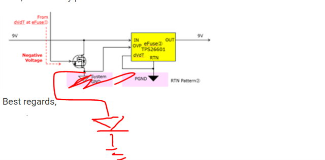
When above case, please let me know about dVdT operation on reverse input supply connection.

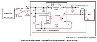
(Condition is Application note: slva934a, page 3)

https://www.ti.com/jp/lit/an/slva934a/slva934a.pdf

They are concerned that if the dVdT voltage swing negative and the gate voltage of the above FET also swing negative, the VGS voltage may exceed the maximum rating.

Best regards,

Satoshi

  • Hi Satoshi,

    Let me check and get back on this.

    Regards

    Kunal Goel

  • Hi Kunal

    Thank you for reply,

    I understood, I looking forward your update.

    Best regards,

    Satoshi

  • Hi Satoshi,

    In case of reverse polarity dvdt-gnd will be negative and RTN to GND will be negative. So VGS = (dvdt-gnd)-(RTN-GND).  RTN-GND should be more negative so overall VGS will be positive. 

    Regards

    Kunal Goel

  • Hi Kunal

    Thank you for reply,

    Sorry for additional question about dVdT, would you please let me know three points below on above (TPS26601 ×2) condition?

    ・Is it okay to separate the RTN (PGND) pattern for the two TPS26601s?

    ・When VIN2 is already supply and VIN connect reverse input supply, is this also no problem?

    ・Customer are considering a circuit that connects dTdV to FPGA in order to determine which TPS26601 is ON.

     Is the circuit below correct?

     Would you let me know if you have any other recommend idea?

    Best regards,

    Satoshi

  • Hi Satoshi,

    1. Yes keeping RTN plane separate for two TPS26601 is fine.

    2.  Yes that should be fine.

    3. This looks fine. They can also use FLT pin for this purpose. Whenever FLT is low that means FET is off.

    Regards

    Kunal Goel

  • Hi Kunal

    Thank you for reply,

    Would you let me confirm about relation for RTN and reverse input connection?

    About condition for RTN plane separate for two TPS26601;

    When one of TPS26601 occur reverse input supply connection, RTN to GND will be negative and fine.

    But I guess the other TPS26601's RTN will not be negative, RTN will GND level. 

    (The other TPS26601's RTN assume to connect another DC/DC's GND)

    Is above thinking correct?

    I concern about RTN plane separate have problem on reverse input connection.


    Best regards,

    Satoshi

  • Hi Satoshi,

    Yes you are right. RTN wrt to GND will be negative when reverse polarity.  But what will be concern if RTN plane seperate? GND will be same for both eFuses?

    Regards

    Kunal Goel

  • Hi Kunal

    Thank you for quick reply,

    Yes, concern point is that GND and board will be not same for both eFuses.

    Best regards,

    Satoshi

  • Sorry Satoshi I am getting confused.

    Are you saying this scenario?

    If you have some block diagram that will help.

    What is the concern? Some damage?

    Regards

    Kunal Goel

  • Hi Kunal

    Sorry for less information,

    Block image is attached, please refer below;

    These are two supply rail and two TPS26601 line, separate RTN(PGND) pattern and common GND pattern. 

    My concern point is damage of the FET on eFuse② side.

    When already 9V supplied and eFuse① line become reverse input connection, RTN pattern① will be negative (VGS = (dvdt-gnd)-(RTN-GND)) and no problem.

    I guess that RTN pattern② will be GND level, not be negative. 

    In this case  I concern about FET swing negative, the VGS voltage may exceed the maximum rating.

    Would you let me confirm that above thinking correct or not.

    Best regards,

    Satoshi

  • Hi Satoshi,

    You are right. Can we connect FET source to system GND and not to RTN plane?

    Regards

    Kunal Goel

  • Hi Kunal

    Thank you for confirming,

    About FET source to system GND, I think that gate voltage will be negative and source voltage will be GND level on reverse input connection. 

    What is the state of system GND?

    Also, is there any problem?

    Best regards,

    Satoshi

  • Hi Satoshi,

    I got your point. You are talking about the case when eFuse 1 input goes negative. In that case eFuse 2 RTN will be connected internally to device GND pin(system gnd).

    So if we connect FET source to RTN2 or SYSTEM GND it will be same for the case when eFuse 1 is facing reverse polarity.

    So yes VGS will be negative.  But I dont think it will go beyond input voltage range. If we can choose FET of VGS rating near max reverse polarity it should be fine. FET can handle both positive and negative VGS.

    Another way to block reverse VGS is to add a diode like this:

    Regards

    Kunal Goel

  • Hi Kunal

    Thank you for information, I understood.

    Another candidate for consideration has been added, which is a configuration that protects the System GND on the eFuse ① side as shown below.

    Is this enough to protected for reverse input connection?

    Would you let me know if you feel impossible, found the revised points, etc.

    Best regards,

    Satoshi

  • Hi Satoshi,

    Looks fine to me.

    Regards

    Kunal Goel