This thread has been locked.

If you have a related question, please click the "Ask a related question" button in the top right corner. The newly created question will be automatically linked to this question.

LM25184-Q1: Worst Case Circuit Analysis: Vout modelling over temperature and related factors

Part Number: LM25184-Q1

Hello Dear TI Team,

We need to provide estimation of the Vout range over temperature in terms of WCCA considering all internal and external variables/factors or in other words to determine the function Vout=f('variation over temperature of all internal current sources and voltage references', RFB, RSET, RTC)

To do that, we first tried to use the PSICE model available on the LM25184-Q1 product page, however it seems incomplete or simplified. We tried also with the updated SPICE model of LM25184-Q1 delivered in that forum 8 Months ago - the same result.

Therefore can you please provide such complete formula for Vout as function of the related internal and external variables, as described above?

Other solution could be more accurate SPICE model of LM25184-Q1, however such approach has additional and hidden risks and uncertainties.

Best regards,

Cvetan Marinov

  • Hi 

    spice model is only behaviour model which don't include any temperature parameters. 

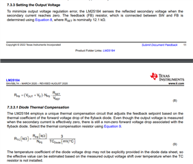
    can you refer below formular to estimate the temperature change impact to the output voltage? 

  • Hello Daniel Li14,

    Thank you.

    However, in order to make a worse case analysis for output voltage tolerance based on the proposed two formulas, we need some clarifications of the datasheet parameters.

    So, can you please clarify the following points:

    1. In the datasheet first page is stated ±1.5% load and line regulation. Is that ±1.5% load regulation plus additional ±1.5% for line regulation, or is it combined ±1.5% for load and line regulation?
    2. For calculating Flyback output voltage is used formula Vout=Rfb*Vref/Rset/Nps-VD. 

    2.1.The value and the tolerance of the "Vref '' parameter is not clear, "Vref" is defined only in the Functional Block Diagram as a trimmed reference, but with no nominal value/tolerance and temperature dependence. Please clarify?

    2.2.In  "7.3.4 Control Loop Error Amplifier'' is mentioned an internal 1.21-V reference set by the resistor at RSET pin, but not clear how to interpret it. 

    2.3.In "6.5 Electrical Characteristics" FEEDBACK fields are defined parameters Irset and Vrset. Please, clarify if Irset and Vrset are dependent from Rset resistor value?

    2.4.In "6.5 Electrical Characteristics" FEEDBACK fields are defined parameters VFB-VIN1 and  VFB-VIN2.  Please, clarify for what these parameters stand for, and if they can influence output voltage tolerance?

    2.5 Please clarify "Figure 6-8. RSET Current versus Temperature"? Is that Rset current in function from Rset resistor tolerance and temperature coefficient?

    2.6. In "6.5 Electrical Characteristics"  DIODE THERMAL COMPENSATION field VTC is defined at  ITC=±10 µA and TJ=25°C with nominal 1.2V and maximum 1.27V. Is there a minimum value, or the whole range can drift is 1.2V-1.27V?

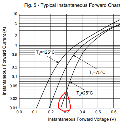
    2.7. VD is definefined as forward voltage drop of the flyback diode as its current approaches zero. Can you specify a diode forward current value at which VD is measured?

    Best regards,

    Cvetan Marinov

  • Hi Cvetan,

    I will check with datasheet and reply you later.

    Thanks

    Colin

  • Hi Colin,

    Are there any updates on my topic so far?

  • Hi Cvetan,

    Sorry for responding late.

    Q1:it is combined ±1.5% for load and line regulation;

    Q2: the Vref=Vset=1.21V;

    Q3:Iset=Vset/Rset= 1.21V/Rset, so it is clear Irset and Vrset are not dependent from Rset resistor value.

    For questions 2.4-2.7, I need check with others and will update sonly.

    Colin

  • Hi Cvetan,

    Q2.2:  There is an internal current source that would build 1.21V across RSET.  

    Q2.3.  Basically, VRSET is 1.21V fixed, and RSET just changes the current pulling through it.  We recommend RSET=12.1k, and do not recommend a different value. If you choose a different RSET, VRSET would still be 1.21V and the internal current source would change in accordance to produce 1.21V across RSET.  Refer to  Equation (8), and you will need to adjust RFB to get your voltage setting point. 

    Q2.4. These are the limitations of the working voltage across the two pins.  Following Equation (8) and setting RSET=12.1k should meet these limits. 

    Q2.5. It is a typical device internal current source tolerance, excluding RSET tolerance.  It reflects the VSET tolerance in the RSET current when RSET=12.1k.   In a real design, you need also to consider the RSET tolerance when assessing your Vout regulation results.

    Q2.6. The min is down to 0.

    Q2.7.  Please check your diode datasheet, and there should be a curve like this, and I marked the VD point:  use the voltage close to ~10mA point. 

    Hope these clarify.

    Best Regards,

    Youhao

  • Hello Colin,

    Thank you for your response.

    Is there any chance to have an updated PSpice model for LM25184-Q1?

    Best regards,

    Cvetan Marinov

  • Hello Youhao Xi,

    Thank you for your response!

    Is there any chance to have an updated PSpice model of LM25184-Q1, which is not just behavioral model?

    Also, may we have a more detailed architectural (functional) Block Diagram of the device?


    Best regards,

    Cvetan Marinov

  • Hi Cvetan,

    We will have the opportunity to update.

    Thanks 

    Colin