Other Parts Discussed in Thread: LM62460, TPSM63606
Hi,
I've designed a new board with LM25148 . I follow the Figure 9-17. Application Circuit from datasheet to do a 3.3VDC/4A power rail.
I choose the following component :
- Self : 2.2µF/15A / 7mOhms max
- Cinput=2*47µF/50V chimical low esr and 2*2.2µF/50V ceramic
- Coutput = 3*47µF ceramic 10V
- PFM/SYNC=VDDA= diode emulation mode
- VCCx=0
- Compensation = approximatively same as evaluation board (10K+4.7nF)//18pF.
- Mosfet : QG=15 to 20nC / Cg=1100pF / VDSS=40V / Rdsmax=30mOhms
- Feed back = RFH = 150K ; RFB=47K (tested with 100K to VDDA too) for 3V3 output
- Cboot = 100nF/50V
- Cvdda=1µF/25V
- Cvcc= 10µF/10V
- En = High = 2.8VDC
- CNFG=41.2K
- RT=41.2K for 525KHz switching
- no low pass filtering on ISNS+ (only kelvin connection)
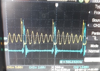
For Iout = 0A to 250mA everything works fine (3V3 with 40mVpk ripple).
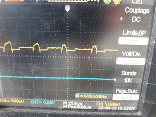
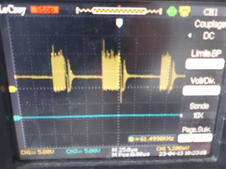
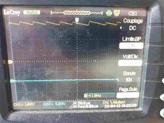
For Iout > 250mA, I've a Vout from 2.8VDC to 3VDC with 500mVpk ripple which seems to be unstable (unlike VDDA and VCC seems to be ok).
I try with the internal compensation too (with 100K to VDDA)
I got the following HO output (blue) and LO (yellow).

I use the excel snvr504b to check design and I didn't see any mistake.
The design is similar to the design generated by the TI webench tool.
Do you've an idea on my mistake ?
Thanks.