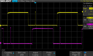
While updating a very early design for the 20 pin version surface mount version of this device, I found a small but important difference in from the 16 pin dual inline package in how the device performed.
I basically had a finished PCB without the outputs of the IC being connected and operating with an 12 V lab supply. When operating at about 100KHz oscillator frequency, the outputs both exhibited a extra 150nS pulse.

All input signals appeared normal. The PWM amplifier was biased so the outputs repained on. So this was basically set up as a breadboard.
After carefully searching for I stumbled across the problem.
It appears that the engineer in the early 1980's decided to dutifully bypass all unused pins to ground. This included to oscillator output pin which was bypassed with 100pF.After removing the capacitor the IC returned to normal operation. This was surprising since this signal directly drove the input to a flip flop that was supposed to latch the output and prevent double pulsing.
In addition, no differences in the internal oscillator were noted on the Test Data sheet for the part. (SLUS191D Feb. 97)
/cfs-file/__key/communityserver-discussions-components-files/196/uc3525a.pdf
Now I am wondering what is the difference between the two parts? The Dual inline package had no problems with the 100 pF capacitor on the Oscillator output pin while the 20 pin surface mount package exhibits this double pulsing.
At least this should be added as a note to the data sheet?

