Hi team,
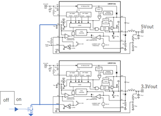
3.3V and 5V are generated with the attached circuit configuration.
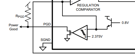
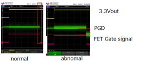
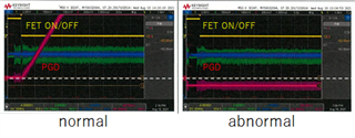
Even though 3.3V is being output, PGD on the 3.3V side does not become High-Z and has a negative voltage.
What causes PGD to be biased to a negative voltage?
Best Regards,
Hi team,
3.3V and 5V are generated with the attached circuit configuration.
Even though 3.3V is being output, PGD on the 3.3V side does not become High-Z and has a negative voltage.
What causes PGD to be biased to a negative voltage?
Best Regards,